コンテンツへスキップ
Merck

920088

Sigma-Aldrich

Graphene, monolayer film

large grain, CVD graphene on copper foil, A5 size

別名:

Roll-to-Roll graphene

ログイン組織・契約価格を表示する


About This Item

化学式:
C
CAS番号:
MDL番号:
UNSPSCコード:
12141908
NACRES:
NA.23
製品920088は現在お客様の国では販売されていません。 製品に関するお問い合わせはこちら(テクニカルサービス)

製品名

R2R Monolayer large grain CVD graphene on copper foil, A5 size, avg. no. of layers, 1

品質水準

詳細

Growth method: roll-to-roll CVD
Raman intensity 2D/G: ≥1.5
Number of layer: Monolayer

特徴

avg. no. of layers 1

シート抵抗

280 Ω/sq ±10%

サイズ

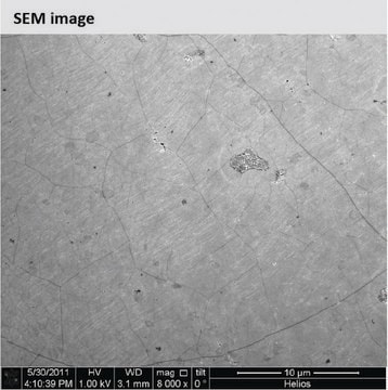
110 μm × 110 μm ± 10%, grain size

厚さ

35 μm , Cu Foil

表面被覆率

surface coverage >98%

透過率

>97%

半導体特性

(mobility>3000 cm2/V·s) (Hall effect measurements)

SMILES記法

NC.NC.NC.NC.NC.NC.NC.NC.NC

InChI

1S/9CH5N/c9*1-2/h9*2H2,1H3

InChI Key

DXIFQVRACSPGSU-UHFFFAOYSA-N

類似した製品をお探しですか? 訪問 製品比較ガイド

関連するカテゴリー

詳細

Roll-to-roll, high-quality, monolayer CVD graphene with large grain size (∼110μm2) on copper foil, A5 size.

アプリケーション

Our Roll-to-Roll CVD graphene products are true monolayer high quality graphene, fabricated inside a Cleanroom, heavily monitored and QC to assure high reproducibility.
The roll-to-roll process allows continuous, large scale graphene production.[1]

This large grain size product with low sheet resistance would enable unmatched reproducibility and allow high performance for CVD graphene based FET[2], CVD graphene based sensors, and heterostructure based micro/nano electronics[3].

Application examples:
  • Ultrafast Transistor
  • Optical devices
  • Bio/Gas Sensor
  • Transparent Electrode
  • Flexible Display
  • Smart Coating
  • Thermal management

注意

Be cautious not to drop
Keep away from contamination, heat, dust and flame etc.

保管および安定性

Avoid direct sun light, avoid high temperature, avoid high humidity, and avoid dust.

法的情報

Product of LG Electronics, R&D use only

ピクトグラム

Environment

シグナルワード

Warning

危険有害性情報

注意書き

危険有害性の分類

Aquatic Acute 1 - Aquatic Chronic 1

保管分類コード

13 - Non Combustible Solids

WGK

WGK 2

引火点(°F)

Not applicable

引火点(℃)

Not applicable


最新バージョンのいずれかを選択してください:

試験成績書(COA)

Lot/Batch Number

It looks like we've run into a problem, but you can still download Certificates of Analysis from our 資料 section.

サポートが必要な場合は、お問い合わせください カスタマーサポート

以前この製品を購入いただいたことがある場合

文書ライブラリで、最近購入した製品の文書を検索できます。

文書ライブラリにアクセスする

Integrating graphene into semiconductor fabrication lines.
Daniel Neumaier et al.
Nature materials, 18(6), 525-529 (2019-05-23)
Hao-Ling Tang et al.
ACS nano, 11(12), 12817-12823 (2017-11-29)
Two-dimensional (2D) materials are drawing growing attention for next-generation electronics and optoelectronics owing to its atomic thickness and unique physical properties. One of the challenges posed by 2D materials is the large source/drain (S/D) series resistance due to their thinness
Bing Deng et al.
Advanced materials (Deerfield Beach, Fla.), 31(9), e1800996-e1800996 (2018-10-03)
Chemical vapor deposition (CVD) is considered to be an efficient method for fabricating large-area and high-quality graphene films due to its excellent controllability and scalability. Great efforts have been made to control the growth of graphene to achieve large domain

資料

グラフェン電界効果トランジスタチップをご紹介します。研究初期での高品質GFETを製造するという負担をかけずに、アプリケーション主導の研究を可能にします。

1D vdWHのレビュー:1D vdWHを使用したデバイスの材料、合成、光電子応用、課題、将来の展望について説明します。

Review on 1D vdWHs: Discusses materials, synthesis, optoelectronic applications, challenges, and future perspectives for 1D vdWH-based devices.

質問

レビュー

評価値なし

アクティブなフィルタ

ライフサイエンス、有機合成、材料科学、クロマトグラフィー、分析など、あらゆる分野の研究に経験のあるメンバーがおります。.

製品に関するお問い合わせはこちら(テクニカルサービス)