
FIPMS223
Back-gated OFET Interdigitated Substrate
Au source/drain, 90 nm SiO2 gate-insulator, varied W/L from 500 to 4000, 16 transistors per chip, chips (diced)
Scegli un formato
1.470,00 €
Scegli un formato
About This Item
1.470,00 €
Prodotti consigliati


Stato
chips (diced)
Confezionamento
pack of 1 (wafer of 60 diced chips)
Temperatura di conservazione
15-25°C
Cerchi prodotti simili? Visita Guida al confronto tra prodotti
Categorie correlate
Descrizione generale
Layer structure:
- Gate: n-doped silicon (doping at wafer surface: n~3x10¹⁷/ cm3)
- Gate oxide: 90 nm ± 10 nm SiO2 (thermal oxidation)
- Drain/source: 30 nm Au with 10 nm high work function adhesion layer (ITO), by lift-off technique
- Protection: resist AR PC 5000/3.1 (soluble in AZ-Thinner or acetone)
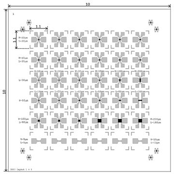
- Layout: see images
- Test chip size: 15 x 15 mm2
- No. of chips: 60 per wafer
- Contact pads: 0.5 x 0.5 mm2
- No. of transistors: 16 per chip
4 x transistors L= 2.5 μm W= 10 mm
4 x transistors L= 5 μm W= 10 mm
4 x transistors L= 10 μm W= 10 mm
4 x transistors L= 20 μm W= 10 mm
Applicazioni
Confezionamento
Nota sulla preparazione
To guarantee a complete cleaning of the wafer / chip surface from resist residuals, please rinse by acetone and then dry the material immediately by nitrogen (compressed air).
Recommendation for material characterization:
If gate currents appear during the characterization of the field effect transistors, considerable variations could occur at the extraction of the carrier mobility. Therefore it is necessary to check the leakage currents over the reverse side (over the chip edges) of the OFET-substrates.
Stoccaggio e stabilità
Resist layer was applied to prevent damage from scratches.
Expiration date is the recommended period for resist removal only. After resist removal, the substrate remains functional and does not expire.
Note legali
Scegli una delle versioni più recenti:
Certificati d'analisi (COA)
It looks like we've run into a problem, but you can still download Certificates of Analysis from our Documenti section.
Se ti serve aiuto, non esitare a contattarci Servizio Clienti
Possiedi già questo prodotto?
I documenti relativi ai prodotti acquistati recentemente sono disponibili nell’Archivio dei documenti.
Articoli
Professors Tokito and Takeda share design principles and optimization protocols for organic electronic devices, focusing on flexibility and low cost.
Filtri attivi
Il team dei nostri ricercatori vanta grande esperienza in tutte le aree della ricerca quali Life Science, scienza dei materiali, sintesi chimica, cromatografia, discipline analitiche, ecc..
Contatta l'Assistenza Tecnica.