Passa al contenuto
Merck
Tutte le immagini(2)

Documenti fondamentali

GRFETS10

Sigma-Aldrich

Graphene FET chip

S10

Sinonimo/i:

Graphene FET, Graphene FET sensor, Graphene FET with 30 Hall-bar devices and 6 2-probe configurations with varied channel geometry

Autenticatiper visualizzare i prezzi riservati alla tua organizzazione & contrattuali

Scegli un formato

1 EA
537,00 €

537,00 €


Per informazioni sulla disponibilità, contatta il Servizio Clienti.

Richiedi un ordine bulk

Scegli un formato

Cambia visualizzazione
1 EA
537,00 €

About This Item

Codice UNSPSC:
43211915
NACRES:
NA.23

537,00 €


Per informazioni sulla disponibilità, contatta il Servizio Clienti.

Richiedi un ordine bulk

Descrizione

Dirac point:< 50 V
Gate Oxide material: SiO2
Gate Oxide thickness: 90 nm
Graphene field-effect mobility: >1000 cm2/V·s
Maximum gate-source voltage: ± 50 V
Maximum temperature rating: 150 °C
Maximum drain-source current density: 107 A/cm2

Metallization: Chromium 2 nm/Gold 50 nm
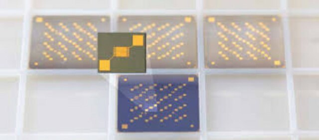
Monolayer CVD grown Graphene based field effect transistors (FET) S10
Residual charge carrier density: <2 x 1012 cm-2
Resistivity of substrate: 1-10 Ω·cm
Yield >75%

Cerchi prodotti simili? Visita Guida al confronto tra prodotti

Descrizione generale

Device configuration:

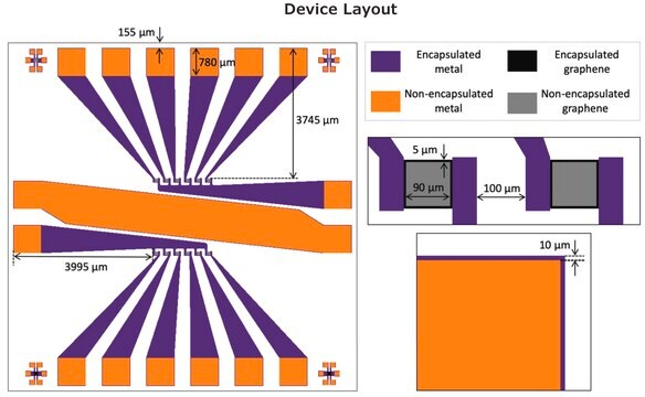
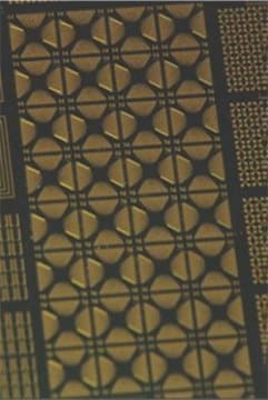
This Graphene FET chip provides 36 graphene devices distributed in a grid pattern on the chip. 30 devices have Hall-bar geometry and 6 have 2-probe geometry.
The Hall-bar devices can be used for Hall measurements as well as 4-probe and 2-probe measurements. There are graphene channels with varied dimensions to allow systematic investigation of device properties.
Graphene FET chip (GFET-S10 chip) is a graphene based field effect transistor chip with a symmetric transconductance of 8 μS and an operational current density of 105 A/cm2. The fabricated device has a monolayered graphene which is coated by chemical vapor deposition (CVD) on silicon substrate. It also has similar gate insulators in the source and drain.[1][2][3]

Applicazioni

  • Graphene device research[4]
  • FET based sensor research for active materials deposited on graphene[5]
  • Chemical sensors[5]
  • Biosensors[6]
  • Bioelectronics[6]
  • Magnetic sensors
  • Photodetectors
GFET-S10 chip can be used as a biosensor and a chemical sensor for biological applications.[7][8]

Caratteristiche e vantaggi

Device Features:

  • State-of-art graphene FETs utilizing consistent high-quality CVD grown monolayer graphene
  • Devices are not encapsulated and can be functionalized by additives
  • Perfect platform for sensor research and development
  • 36 individual graphene FETs per chip
  • Mobilities typically > 1000 cm2/V·s

Avvertenza

Basic handling instructions:The monolayer CVD graphene used in this FET device is highly prone to damage by external factors.
To maintain the quality of the devices, we recommend taking the following precautions:
  • Be careful when handling the graphene FET chip.
  • Tweezers should not contact the device area directly.

Codice della classe di stoccaggio

11 - Combustible Solids

Classe di pericolosità dell'acqua (WGK)

nwg

Punto d’infiammabilità (°F)

Not applicable

Punto d’infiammabilità (°C)

Not applicable


Scegli una delle versioni più recenti:

Certificati d'analisi (COA)

Lot/Batch Number

It looks like we've run into a problem, but you can still download Certificates of Analysis from our Documenti section.

Se ti serve aiuto, non esitare a contattarci Servizio Clienti

Possiedi già questo prodotto?

I documenti relativi ai prodotti acquistati recentemente sono disponibili nell’Archivio dei documenti.

Visita l’Archivio dei documenti

I clienti hanno visto anche

Slide 1 of 2

1 of 2

Graphene amine functionalized, avg. no. of layers, 1 &#8209; 5

Sigma-Aldrich

900551

Graphene

Graphene silane modified, avg. no. of layers, 1 &#8209; 5

Sigma-Aldrich

900552

Graphene

Wafer-scale statistical analysis of graphene field-effect transistors-part II: analysis of device properties
Smith A D, et al.
IEEE Transactions on Electron Devices, 64(9), 3927-3933 (2017)
Review-Field-Effect Transistor Biosensing: Devices and Clinical Applications
Syu Y C, et al.
ECS journal of solid state science and technology : JSS, 7(7), Q3196-Q3207 (2018)
MoS2-graphene heterostructures as efficient organic compounds sensing 2D materials
Pham T, et al.
Carbon, 142, 504-512 (2019)
Jeffrey Abbott et al.
Methods in molecular biology (Clifton, N.J.), 1572, 169-187 (2017-03-17)
Electrical sensing of biomolecules has been an important pursuit due to the label-free operation and chip-scale construct such sensing modality can enable. In particular, electrical biomolecular sensors based on nanomaterials such as semiconductor nanowires, carbon nanotubes, and graphene have demonstrated
High-kappa Solid-Gate Transistor Configured Graphene Biosensor with Fully Integrated Structure and Enhanced Sensitivity
Wang C, et al.
Advances in Functional Materials, 26(42), 7668-7678 (2016)

Articoli

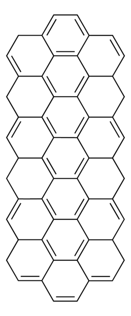
Graphene nanoribbons (GNRs) are quasi-one-dimensional narrow strips of graphene comprised of sp2-hybridized carbon atoms arranged into hexagonal honeycomb lattice configurations.

Domande

Recensioni

Nessuna valutazione

Filtri attivi

Il team dei nostri ricercatori vanta grande esperienza in tutte le aree della ricerca quali Life Science, scienza dei materiali, sintesi chimica, cromatografia, discipline analitiche, ecc..

Contatta l'Assistenza Tecnica.