


The S20 device is designed for biosensing, while the S10 model is recommended for detecting other chemicals.
推薦產品
描述
Absolute Maximum Ratings
Maximum gate-source voltage: ± 50 V
Maximum temperature rating: 150 °C
Maximum drain-source current density: 107 A/cm2
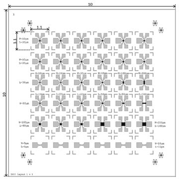
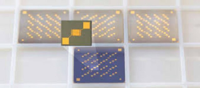
Chip dimensions: 10 mm x 10 mm
Chip thickness: 675 μm
Dirac point: < 50 V
Yield >75%
Encapsulation: 50 nm Al2O3 + 100 nm Si3N4
Gate oxide materials: 90 nm SiO2
Graphene field-effect mobility: >1000 cm2/V·s
Monolayer CVD grown Graphene based 2-probe field effect transistors (FET).
Number of devices per chip: 12
Resistivity of substrate: 1-10 Ω·cm
Metallization: Chromium/Gold-Palladium 2/50 nm
尋找類似的產品? 前往 產品比較指南
一般說明
Device configuration:
The graphene FET-S20 chip is designed for measurements in liquid medium. This chip provides 12 graphene devices, with encapsulation on the metal pads to avoid degradation and reduce leakage currents, and the probe pads located near the periphery of the chip. It also includes a non-encapsulated electrode at the center of the chip, which allows liquid gating without the need of an external gate electrode.
The graphene FET-S20 chip is designed for measurements in liquid medium. This chip provides 12 graphene devices, with encapsulation on the metal pads to avoid degradation and reduce leakage currents, and the probe pads located near the periphery of the chip. It also includes a non-encapsulated electrode at the center of the chip, which allows liquid gating without the need of an external gate electrode.
應用
特點和優勢
Device Features:
- State-of-the-art GFETs utilizing consistently high-quality CVD monolayer graphene
- Metallic contacts and metal/graphene interface are encapsulated to avoid degradation and reduce leakage current in liquid environment
- Perfect platform device for new sensor research and development
- 12 individual GFETs per chip
- A central gate electrode
儲存類別代碼
11 - Combustible Solids
水污染物質分類(WGK)
nwg
閃點(°F)
Not applicable
閃點(°C)
Not applicable
Graphene field effect transistors on flexible substrate: stable process and high RF performance
2016 11th European microwave integrated circuits conference, 7(1), 165-168 (2016)
Improved sensitivity of a graphene FET biosensor using porphyrin linkers
Kawata T, et al.
Japanese Journal of Applied Physics, 57(6), 065103/1-065103/4 (2018)
Michael T Hwang et al.
Advanced materials (Deerfield Beach, Fla.), e1802440-e1802440 (2018-07-10)
Electronic DNA-biosensor with a single nucleotide resolution capability is highly desirable for personalized medicine. However, existing DNA-biosensors, especially single nucleotide polymorphism (SNP) detection systems, have poor sensitivity and specificity and lack real-time wireless data transmission. DNA-tweezers with graphene field effect
MoS2-graphene heterostructures as efficient organic compounds sensing 2D materials
Pham T, et al.
Carbon, 142, 504- 512 (2019)
Review-Field-Effect Transistor Biosensing: Devices and Clinical Applications
Syu Y C, et al.
ECS journal of solid state science and technology : JSS, 7(7), Q3196-Q3207 (2018)
文章
Graphene nanoribbons (GNRs) are quasi-one-dimensional narrow strips of graphene comprised of sp2-hybridized carbon atoms arranged into hexagonal honeycomb lattice configurations.
-
Can the GFET-S20 Graphene FET chip be used in air or vacuum environments for detecting other chemicals?
1 answer-
Helpful?
-
Active Filters
我們的科學家團隊在所有研究領域都有豐富的經驗,包括生命科學、材料科學、化學合成、色譜、分析等.
聯絡技術服務