推薦產品
形狀
chips (diced)
包裝
pack of 1 (wafer of 60 diced chips)
儲存溫度
15-25°C
尋找類似的產品? 前往 產品比較指南
一般說明
Substrate: 150 mm wafer according to semiconductor standard (used for bottom-gate)
Layer structure:
4 x transistors L= 2.5 μm W= 10 mm
4 x transistors L= 5 μm W= 10 mm
4 x transistors L= 10 μm W= 10 mm
4 x transistors L= 20 μm W= 10 mm
Layer structure:
- Gate: n-doped silicon (doping at wafer surface: n~3x10¹⁷/ cm3)
- Gate oxide: 90 nm ± 10 nm SiO2 (thermal oxidation)
- Drain/source: 30 nm Au with 10 nm high work function adhesion layer (ITO), by lift-off technique
- Protection: resist AR PC 5000/3.1 (soluble in AZ-Thinner or acetone)
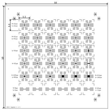
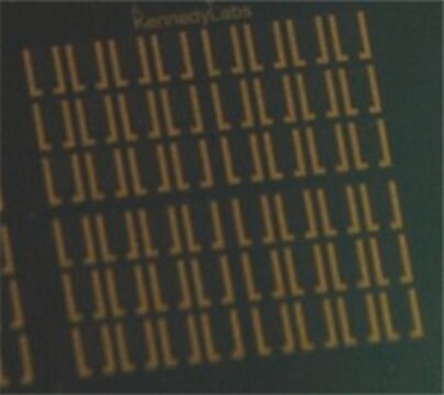
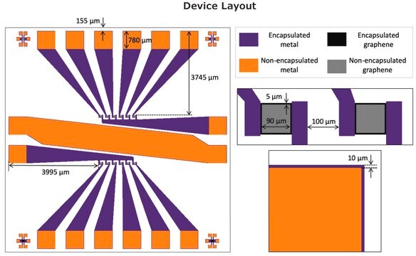
- Layout: see images
- Test chip size: 15 x 15 mm2
- No. of chips: 60 per wafer
- Contact pads: 0.5 x 0.5 mm2
- No. of transistors: 16 per chip
4 x transistors L= 2.5 μm W= 10 mm
4 x transistors L= 5 μm W= 10 mm
4 x transistors L= 10 μm W= 10 mm
4 x transistors L= 20 μm W= 10 mm
應用
Back-gated OFET Interdigitated Substrate (organic field-effect transistor) can be used in the fabrication of chemical sensors for potential usage in pH sensing and detection of immunoassays. It can also be used in the fabrication of biosensors by coating the sheets of the FET with a specific antibody for the detection of SARS-CoV-2. FET based biosensors can be potentially used in clinical diagnosis, point of care testing, and on-site detection.
包裝
diced wafer on foil with air tight packaging
準備報告
Recommendation for resist removal:
To guarantee a complete cleaning of the wafer / chip surface from resist residuals, please rinse by acetone and then dry the material immediately by nitrogen (compressed air).
Recommendation for material characterization:
If gate currents appear during the characterization of the field effect transistors, considerable variations could occur at the extraction of the carrier mobility. Therefore it is necessary to check the leakage currents over the reverse side (over the chip edges) of the OFET-substrates.
儲存和穩定性
Store the wafers at a cool and dark place and protect them against sun.
Resist layer was applied to prevent damage from scratches.
Expiration date is the recommended period for resist removal only. After resist removal, the substrate remains functional and does not expire.
Resist layer was applied to prevent damage from scratches.
Expiration date is the recommended period for resist removal only. After resist removal, the substrate remains functional and does not expire.
法律資訊
Product of Fraunhofer IPMS
分析證明 (COA)
輸入產品批次/批號來搜索 分析證明 (COA)。在產品’s標籤上找到批次和批號,寫有 ‘Lot’或‘Batch’.。
Rapid detection of COVID-19 causative virus (SARS-CoV-2) in human nasopharyngeal swab specimens using field-effect transistor-based biosensor
Seo G, et al.
ACS Nano, 14(4), 5135-5142 (2020)
The impact of biosensing in a pandemic outbreak: COVID-19
Morales-Narvaez E and Dincer C
Biosensors And Bioelectronics, 14(4), 112274-112274 (2020)
Polymer composite-based OFET sensor with improved sensitivity towards nitro based explosive vapors
Dudhe RS, et al.
Sensors and Actuators B, Chemical, 148(1), 158-165 (2010)
Random CNT network and regioregular poly (3-hexylthiophen) FETs for pH sensing applications: A comparison
Munzer AM, et al.
Biochim. Biophys. Acta Gen. Subj., 1830(9), 4353-4358 (2013)
文章
Professors Tokito and Takeda share design principles and optimization protocols for organic electronic devices, focusing on flexibility and low cost.
我們的科學家團隊在所有研究領域都有豐富的經驗,包括生命科學、材料科學、化學合成、色譜、分析等.
聯絡技術服務


