


Graphene should be on top of the Cu foil. Since graphene has PMMA protection, a simple way is to start the Cu etching and see which side the Cu foil is on.
Przejdź do
900445

Graphene, monolayer film

Bardziej ekologiczna alternatywa
1 in x 1 in on copper foil, with PMMA coating, avg. no. of layers, 1
Synonim(y):
PMMA/Graphene/Cu
Zaloguj się, aby wyświetlić ceny organizacyjne i kontraktowe.
Informacje o tej pozycji
UNSPSC Code:
12141908
NACRES:
NA.23
Nazwa produktu
Monolayer graphene film, 1 in x 1 in on copper foil, with PMMA coating, avg. no. of layers, 1
description
Film Coverage: >98%, Monolayer coverage: ≥92% (optical)
form
film
quality
Raman analysis-monolayer
feature
avg. no. of layers 1
greener alternative product characteristics
Design for Energy Efficiency
Learn more about the Principles of Green Chemistry.
sustainability
Greener Alternative Product
impurities
<2% (optical)
greener alternative category
General description
We are committed to bringing you Greener Alternative Products that adhere to one of the four categories of Greener Alternatives. This enabling product synthesizes 2D materials with thin layers and high purity, enhancing applications in energy generation, transport, and storage while promoting sustainable practices. Click here for more information.
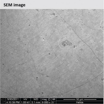
A single-layer graphene film on a copper substrate.
This product is provided with a PMMA coating on top of the graphene in order to ease the transfer process and to avoid contamination. It′s a high quality product with great homogeneity.
Graphene film
Substrate Cu Foil
PMMA Coating
This product is provided with a PMMA coating on top of the graphene in order to ease the transfer process and to avoid contamination. It′s a high quality product with great homogeneity.
Graphene film
- Growth method: CVD synthesis
- Appearance: Transparent film
- Transparency: > 97%
- Coverage: > 95%
- Number of graphene layers: 1
- Thickness (theoretical): 0.345 nm
- FET Electron Mobility on Al2O3: 2000 cm2/Vs
- FET Electron Mobility on SiO2/Si: 4000 cm2/Vs
- Sheet Resistance on SiO2/Si: 450±40 Ω/sq (1cm x1cm)
- Grain size: Up to 10 μm
Substrate Cu Foil
- Thickness: 18 μm
- Pre-treated for easier bottom layer removal: monolayer graphene on the back side of copper is partially removed, but not completely. Therefore, an additional treatment like RIE is needed before transfer to eliminate the bottom layer totally.
PMMA Coating
- Spin coated for high homogeneity
- Molecular weight: 495k
- Thickness: <100 nm
- PMMA model: 495K, A2
Application
- Graphene research
- Flexible batteries
- Electronics
- Aerospace industry
- MEMS and NEMS
- Micro actuators
- Conductive coatings
Ta strona może zawierać tekst przetłumaczony maszynowo.
1 of 1
Ta pozycja | |||
|---|---|---|---|
| description 1 in x 1 in on copper foil, with PMMA coating, avg. no. of layers, 1 | description 1 cm x 1 cm on copper foil, with PMMA coating, avg. no. of layers, 1 | description 10 cm x 10 cm on copper foil, avg. no. of layers, 1 | description 1 cm x 1 cm on SiO2/Si substrate, avg. no. of layers, 1 |
| greener alternative category | greener alternative category | greener alternative category | greener alternative category - |
| sustainability Greener Alternative Product | sustainability Greener Alternative Product | sustainability Greener Alternative Product | sustainability - |
| form film | form film | form film | form film |
| feature avg. no. of layers 1 | feature avg. no. of layers 1 | feature avg. no. of layers 1 | feature avg. no. of layers 1 |
| greener alternative product characteristics Design for Energy Efficiency | greener alternative product characteristics Design for Energy Efficiency | greener alternative product characteristics Design for Energy Efficiency | greener alternative product characteristics - |
| impurities <2% (optical) | impurities <2% | impurities - | impurities - |
Still not finding the right product?
Explore all of our products under Monolayer graphene film
Klasa składowania
13 - Non Combustible Solids
wgk
WGK 2
flash_point_f
Not applicable
flash_point_c
Not applicable
Wybierz jedną z najnowszych wersji:
Masz już ten produkt?
Dokumenty związane z niedawno zakupionymi produktami zostały zamieszczone w Bibliotece dokumentów.
-
Hi, can I know which side of the copper foil has a monolayer graphene? Is it facing up or down? I just wanted to make sure before I use it.
1 answer-
Helpful?
-