コンテンツへスキップ
Merck

911135

Sigma-Aldrich

TU-3

別名:

4,4′-(2λ4δ2-benzo[1,2-c:4,5-c′]bis[1,2,5]thiadiazole-4,8-diyldi-5,2-thiophenediyl)bis[2-dodecylbenzonitrile], 4,8-Bis [5-(4-cyano-3-alkylphenyl)-2-thienyl] benzo[1,2-c:4,5-c′] bis [1,2,5] thiadiazole

ログイン組織・契約価格を表示する


About This Item

実験式(ヒル表記法):
C52H60N6S4
CAS番号:
分子量:
897.33
UNSPSCコード:
12352103
NACRES:
NA.23

詳細

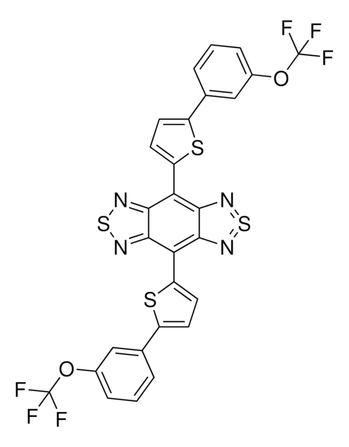
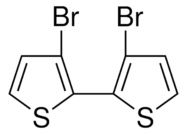
Decomposition temperature: 371 °C (Decomposition start temperature)
mobility = 2.3 cm2 / Vs (@Vsd=100V)
on / off ratio = 107
Structure: BG-TC @ SiO2 / Si
electrode: Au
film: TU-3 / CHCl3 spin coat

アッセイ

≥99% (HPLC)

フォーム

powder

分子量

897.33 g/mol

dark green

mp

291 °C

保管温度

2-8°C

アプリケーション

TU-3 is a n-type organic semiconductor material with long term (year-long) stability in air.[1] And it can be deposited from its solutions to form felxible integrated circuits in either 2D[2][1][3][4] or 3D configurations.[1]
This material achieves a high electron mobility of 2.3 cm2/Vs or more in transistors, making it highly suitable for this application. The mobility of amorphous silicon used in general LCDs and other applications is about 0.5-1cm2/Vs.

法的情報

Organic thin film transistor containing benzobis(thiadiazole) derivatives for organic electronic device by Tanaka, Yasuhiro; Kakita, Kazunari; Machida, Toshikazu From Jpn. Kokai Tokkyo Koho (2017), JP 2017079319 A 20170427.

保管分類コード

11 - Combustible Solids

WGK

WGK 3

引火点(°F)

Not applicable

引火点(℃)

Not applicable


最新バージョンのいずれかを選択してください:

試験成績書(COA)

Lot/Batch Number

It looks like we've run into a problem, but you can still download Certificates of Analysis from our 資料 section.

サポートが必要な場合は、お問い合わせください カスタマーサポート

以前この製品を購入いただいたことがある場合

文書ライブラリで、最近購入した製品の文書を検索できます。

文書ライブラリにアクセスする

A Unique Solution-Processable n-Type Semiconductor Material Design for High-Performance Organic Field-Effect Transistors
Mamada, et al.
Chemistry of Materials, 27, 141-141 (2015)
Yasunori Takeda et al.
Scientific reports, 6, 25714-25714 (2016-05-10)
Ultrathin electronic circuits that can be manufactured by using conventional printing technologies are key elements necessary to realize wearable health sensors and next-generation flexible electronic devices. Due to their low level of power consumption, complementary (CMOS) circuits using both types
Organic Complementary Inverter Circuits Fabricated with Reverse Offset Printing
Takeda Y, et al.
Advanced Electronic Materials, 4(1), 1700313-1700313 (2018)
Compact Organic Complementary D-Type Flip-Flop Circuits Fabricated with Inkjet Printing
Kazuma H, et al
Advanced Electronic Materials, 3(9), 1700208-1700208 (2019)
Jimin Kwon et al.
Nature communications, 10(1), 54-54 (2019-01-04)
Direct printing of thin-film transistors has enormous potential for ubiquitous and lightweight wearable electronic applications. However, advances in printed integrated circuits remain very rare. Here we present a three-dimensional (3D) integration approach to achieve technology scaling in printed transistor density

資料

Professors Tokito and Takeda share design principles and optimization protocols for organic electronic devices, focusing on flexibility and low cost.

時任教授と竹田教授が、プリントおよび溶液処理された、低コストで高度にフレキシブルな有機エレクトロニクスデバイスのための、新しい材料、デバイス構造設計の原則、および性能最適化のプロトコルを紹介します。

関連コンテンツ

有機エレクトロニクスは、有機導電体や有機半導体を用いて、有機太陽電池、有機EL、有機電界効果トランジスタなどの応用実現を目指す分野です。

Organic electronics utilizes organic conductors and semiconductors for applications in organic photovoltaics, organic light-emitting diodes, and organic field-effect transistors.

質問

レビュー

評価値なし

アクティブなフィルタ

ライフサイエンス、有機合成、材料科学、クロマトグラフィー、分析など、あらゆる分野の研究に経験のあるメンバーがおります。.

製品に関するお問い合わせはこちら(テクニカルサービス)