推荐产品
形狀
film
特點
avg. no. of layers 1
電阻
600 Ω/sq
長度 × 寬度 × 厚度
1 cm × 1 cm × (theoretical) 0.345 nm, Monolayer graphene film
1.5 cm × 1.5 cm × 25 μm, copper foil substrate
正在寻找类似产品? 访问 产品对比指南
一般說明
Growth Method: CVD synthesis
Transfer Method: Clean transfer method
Quality Control: Optical Microscopy & Raman checked
Size: 1 cm x 1 cm
Appearance (Color): Transparent
Transparency: >97%
Appearance (Form): Film
Coverage: >95%
Number of graphene layers: 1
Thickness (theoretical): 0.345 nm
FET Electron Mobility on Al2O3: 2; 000 cm2/V·s
FET Electron Mobility on SiO2/Si (expected): 4; 000 cm2/V·s
Sheet Resistance: 600 Ohms/sq.
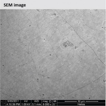
Grain size: Up to 10 μm
Substrate Copper Foil
Thickness: 25μm
Both sides: Graphene/Cu/Graphene
Packaging - 4 units/pack
訊號詞
Warning
危險聲明
危險分類
Eye Irrit. 2 - STOT SE 3
標靶器官
Respiratory system
儲存類別代碼
13 - Non Combustible Solids
水污染物質分類(WGK)
WGK 3
閃點(°F)
Not applicable
閃點(°C)
Not applicable
其他客户在看
商品
Fluorescence quenching microscopy visualizes 2D materials like graphene and MoS2 rapidly, inexpensively, and with high fidelity.
Recent demand for electric and hybrid vehicles, coupled with a reduction in prices, has caused lithium-ion batteries (LIBs) to become an increasingly popular form of rechargeable battery technology.
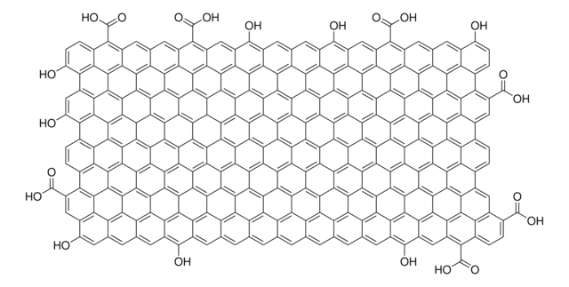
Graphene's unique properties spark interdisciplinary interest; its honeycomb structure offers electrical, optical, and mechanical marvels.
我们的科学家团队拥有各种研究领域经验,包括生命科学、材料科学、化学合成、色谱、分析及许多其他领域.
联系技术服务部门
