推荐产品
product name
Easy transfer monolayer Graphene, L × W 1 in. × 1 in., avg. no. of layers, 1
特點
avg. no. of layers 1
增長模式
CVD
薄層電阻
450 +/- 40 Ω/sq, on SiO2/Si (1cm x 1cm)
長度 × 寬度
1 in. × 1 in.
表面覆盖率
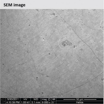
>98%
顏色
transparent>97%
粒徑
≤20 μm
正在寻找类似产品? 访问 产品对比指南
一般說明
A 1 in x 1 in CVD grown monolayer CVD graphene (verified by Raman 2D/G ratio) is sandwiched between a scarificial layer and a water-releasable polymer support film.
Structure of the easy-transfer graphene:
Top sacrificial layer (square shaped), CVD monolayer graphene in the middle, and bottom water-releasable polymer support layer (round shaped)
Structure of the easy-transfer graphene:
Top sacrificial layer (square shaped), CVD monolayer graphene in the middle, and bottom water-releasable polymer support layer (round shaped)
應用
A clean way to trasfer monolayer graphene is highly desired for the utilization of its exceptional properties.
This product employs a specially designed mechanism for easy and clean transfer of high quality monolayer CVD grown graphene to build state-of-art electronic devices such as:
Clean tranfer can be done following below 3 easy steps:
Release
Put the sample on deionized(DI) water slowly, round side (polymer layer) facing down, the square-shaped sacrificial layer+graphene will gradually detach from the rorund polymer film. Once the sacrificial layer/graphene is floating remove the round polymer film.
Transfer
Bring the desired substrate into the same DI water container while the sacrificial layer/graphene is floating. Tilt the substrate 45º and bring it into contact with the sacrificial layer/graphene from below. Take the sacrificial layer/graphene/substrate out and let it dry for 30 minutes in air. Then anneal the samples on a hot plate at 150 Celsius for 1h. Finally, before removing the sacrificial layer, store it under vacuum for at least 24h to avoid detachment of the graphene from your substrate.
Sacrificial layer Removal
To remove the sacrificial layer two methods can be used:
Solvents: Dip the sacrificial layer/graphene/substrate in acetone for 1h, then into isopropyl alcohol for another 1h and blow the sample with N2 to dry it.
Thermal treatment: Put the sacrificial layer/graphene/substrate into an oven and heat the sample at 450 C in
inert atmosphere for 2h.
This product employs a specially designed mechanism for easy and clean transfer of high quality monolayer CVD grown graphene to build state-of-art electronic devices such as:
- Graphene based state-of-art FET
- Graphene based sensors
- Heterostructure based micro/nano electronics
Clean tranfer can be done following below 3 easy steps:
Release
Put the sample on deionized(DI) water slowly, round side (polymer layer) facing down, the square-shaped sacrificial layer+graphene will gradually detach from the rorund polymer film. Once the sacrificial layer/graphene is floating remove the round polymer film.
Transfer
Bring the desired substrate into the same DI water container while the sacrificial layer/graphene is floating. Tilt the substrate 45º and bring it into contact with the sacrificial layer/graphene from below. Take the sacrificial layer/graphene/substrate out and let it dry for 30 minutes in air. Then anneal the samples on a hot plate at 150 Celsius for 1h. Finally, before removing the sacrificial layer, store it under vacuum for at least 24h to avoid detachment of the graphene from your substrate.
Sacrificial layer Removal
To remove the sacrificial layer two methods can be used:
Solvents: Dip the sacrificial layer/graphene/substrate in acetone for 1h, then into isopropyl alcohol for another 1h and blow the sample with N2 to dry it.
Thermal treatment: Put the sacrificial layer/graphene/substrate into an oven and heat the sample at 450 C in
inert atmosphere for 2h.
The material of the sacrificial layer is an Acrylate Based Polymer. The layer is 100 nm thick. The polymeric substrate is a 100 μm thick porous polymeric material.
儲存類別代碼
11 - Combustible Solids
水污染物質分類(WGK)
WGK 1
閃點(°F)
Not applicable
閃點(°C)
Not applicable
商品
Review on 1D vdWHs: Discusses materials, synthesis, optoelectronic applications, challenges, and future perspectives for 1D vdWH-based devices.
我们的科学家团队拥有各种研究领域经验,包括生命科学、材料科学、化学合成、色谱、分析及许多其他领域.
联系技术服务部门


