
推薦產品


產品名稱
单层石墨烯薄膜, 1 cm x 1 cm on quartz, avg. no. of layers, 1
品質等級
形狀
film
特點
avg. no. of layers 1
電阻
600 Ω/sq
長度 × 寬度 × 厚度
1 cm × 1 cm × (theoretical) 0.345 nm, monolayer graphene film
1.25 cm × 1.25 cm × 525 μm, quartz substrate
尋找類似的產品? 前往 產品比較指南
一般說明
Graphene is a unique one atom thick, two dimensional allotrope of carbon. Among all the synthesis technique, chemical vapor deposition of graphene on various substrates is the most promising route for the large scale production of good quality graphene. Graphene deposited on dielectric surface may exhibit better performance in graphene based FETs. Graphene deposited on quartz may be deposited by direct chemical vapor deposition via a sacrificial copper film.
Growth Method: CVD synthesis
Transfer Method: Clean transfer method
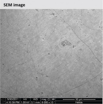
Quality Control: Optical Microscopy & Raman checked
Size: 1 cm x 1 cm
Appearance (Color): Transparent
Transparency: >97%
Appearance (Form): Film
Coverage: >95%
Number of graphene layers: 1
Thickness (theoretical): 0.345 nm
FET Electron Mobility on Al2O3: 2; 000 cm2/V·s
FET Electron Mobility on SiO2/Si (expected): 4; 000 cm2/V·s
Sheet Resistance: 600 Ohms/sq.
Grain size: Up to 10 μm
Substrate Quartz
Size: 1.25 cm x 1.25 cm
Flatness: bow: 20μm; warp: 30μm
Roughness:6 angstroms (on the polished side)
Surface: Double side polished
Transfer Method: Clean transfer method
Quality Control: Optical Microscopy & Raman checked
Size: 1 cm x 1 cm
Appearance (Color): Transparent
Transparency: >97%
Appearance (Form): Film
Coverage: >95%
Number of graphene layers: 1
Thickness (theoretical): 0.345 nm
FET Electron Mobility on Al2O3: 2; 000 cm2/V·s
FET Electron Mobility on SiO2/Si (expected): 4; 000 cm2/V·s
Sheet Resistance: 600 Ohms/sq.
Grain size: Up to 10 μm
Substrate Quartz
Size: 1.25 cm x 1.25 cm
Flatness: bow: 20μm; warp: 30μm
Roughness:6 angstroms (on the polished side)
Surface: Double side polished
應用
Graphene may be extensively incorporated in several applications, such as; nanoelectronics, fuel cells, solar cell, photovoltaic devices, in biosensing, optical biosensors, MEMS, NEMS, field effect transistors (FETs), chemical sensors, nanocarriers in biosensing assays., 4


訊號詞
Danger
危險分類
Carc. 1B - Eye Irrit. 2 - STOT RE 1 Inhalation - STOT SE 3
標靶器官
Lungs, Respiratory system
儲存類別代碼
6.1D - Non-combustible acute toxic Cat.3 / toxic hazardous materials or hazardous materials causing chronic effects
水污染物質分類(WGK)
WGK 3
閃點(°F)
Not applicable
閃點(°C)
Not applicable
Enhancing the conductivity of transparent graphene films via doping
Nanotechnology, 21, 285205/1-285205/6 (2010)
Direct Chemical Vapor Deposition of Graphene on Dielectric Surfaces
Ismach A, et al.
Nano Letters, 10, 1542?1548-1542?1548 (2010)
Optical nano-imaging of gate-tunable graphene plasmons
Nature (2012)
Weak mismatch epitaxy and structural feedback in graphene growth on copper foil.
Wilson NR, et al.
Nano Research, 6(2), 99-112 null
Functionalized CVD monolayer graphene for label-free impedimetric biosensing
Eissa S, et al.
Nano Research, 8(5), 1698-1709 null
文章
生物標誌物的檢測和量化對於醫療診斷、環境監控和生物研究是非常重要的。
Professors summarize recent 2D materials synthesis advancements and biosensing applications in various fields.
近期對於電動車和混合動力車的需求,加上價格的降低,使得鋰離子電池 (LIB) 成為越來越受歡迎的充電電池技術。
我們的科學家團隊在所有研究領域都有豐富的經驗,包括生命科學、材料科學、化學合成、色譜、分析等.
聯絡技術服務