
推荐产品


描述
Dirac point:< 50 V
Gate Oxide material: SiO2
Gate Oxide thickness: 90 nm
Graphene field-effect mobility: >1000 cm2/V·s
Maximum gate-source voltage: ± 50 V
Maximum temperature rating: 150 °C
Maximum drain-source current density: 107 A/cm2
Metallization: Chromium 2 nm/Gold 50 nm
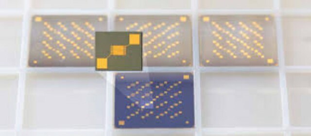
Monolayer CVD grown Graphene based field effect transistors (FET) S10
Residual charge carrier density: <2 x 1012 cm-2
Resistivity of substrate: 1-10 Ω·cm
Yield >75%
正在寻找类似产品? 访问 产品对比指南
一般描述
Device configuration:
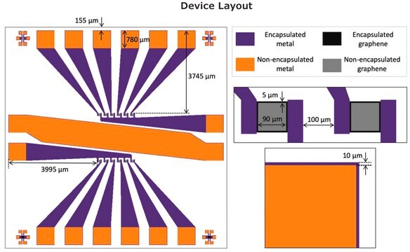
This Graphene FET chip provides 36 graphene devices distributed in a grid pattern on the chip. 30 devices have Hall-bar geometry and 6 have 2-probe geometry.
The Hall-bar devices can be used for Hall measurements as well as 4-probe and 2-probe measurements. There are graphene channels with varied dimensions to allow systematic investigation of device properties.
Graphene FET chip (GFET-S10 chip) is a graphene based field effect transistor chip with a symmetric transconductance of 8 μS and an operational current density of 105 A/cm2. The fabricated device has a monolayered graphene which is coated by chemical vapor deposition (CVD) on silicon substrate. It also has similar gate insulators in the source and drain.[1][2][3]
应用
特点和优势
Device Features:
- State-of-art graphene FETs utilizing consistent high-quality CVD grown monolayer graphene
- Devices are not encapsulated and can be functionalized by additives
- Perfect platform for sensor research and development
- 36 individual graphene FETs per chip
- Mobilities typically > 1000 cm2/V·s
注意
Basic handling instructions:The monolayer CVD graphene used in this FET device is highly prone to damage by external factors.
To maintain the quality of the devices, we recommend taking the following precautions:
To maintain the quality of the devices, we recommend taking the following precautions:
- Be careful when handling the graphene FET chip.
- Tweezers should not contact the device area directly.
储存分类代码
11 - Combustible Solids
WGK
nwg
闪点(°F)
Not applicable
闪点(°C)
Not applicable
其他客户在看
Lanthanide complexes as molecular dopants for realizing air-stable n-type graphene logic inverters with symmetric transconductance
Gajarushi AS, et al.
Materials Horizons, 6(4), 743-750 (2019)
Graphene field effect transistors on flexible substrate: stable process and high RF performance
2016 11th European microwave integrated circuits conference, 7(1), 165-168 (2016)
Wafer-scale statistical analysis of graphene field-effect transistors-part II: analysis of device properties
Smith A D, et al.
IEEE Transactions on Electron Devices, 64(9), 3927-3933 (2017)
Review-Field-Effect Transistor Biosensing: Devices and Clinical Applications
Syu Y C, et al.
ECS journal of solid state science and technology : JSS, 7(7), Q3196-Q3207 (2018)
MoS2-graphene heterostructures as efficient organic compounds sensing 2D materials
Pham T, et al.
Carbon, 142, 504-512 (2019)
商品
Graphene nanoribbons (GNRs) are quasi-one-dimensional narrow strips of graphene comprised of sp2-hybridized carbon atoms arranged into hexagonal honeycomb lattice configurations.
Active Filters
我们的科学家团队拥有各种研究领域经验,包括生命科学、材料科学、化学合成、色谱、分析及许多其他领域.
联系客户支持