
推荐产品


产品名称
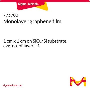
Monolayer Graphene on Si/SiO2 wafer, diam. 100 mm (4 in.)
描述
Graphene Coverage: 100% with sporadic adlayers
Metal Impurities: 1.00e10 – 5.00e10 (at/cm) substrate
Monolayer Graphene Transparency: >97%
Raman D/G ratio: Indistinguishable to 0.03
Substrate Type/Doping: P/B
430 Ω/sq ±50 Ω/sq
质量水平
电阻率
1-10 Ω-cm
直径
100 mm (4 in.)
晶粒度
>40 μm
半导体性质
(mobility>2700 cm2/V·s) (FET mobility)
SMILES字符串
[C]
InChI
1S/C
InChI key
OKTJSMMVPCPJKN-UHFFFAOYSA-N
一般描述
Each graphene unit sold is accompanied by a specification sheet unique to the S/N and contains batch-specific metrics. This eliminates guesswork and ensures that you only get the best, well-characterized, and QA-passed graphene.
应用
Graphene is one of the most promising carbon nanomaterials, and it was first isolated in 2004 by Novoselov, Geim et al,[1] leading to a Nobel prize. It consists of a two-dimensional single layer of sp2 hybridized carbon with hexagonal lattice. It has attracted significant attention in the field of high-performance electronic devices because of its excellent electronic [2] and chemical properties, and large specific surface area [3] . Among the main potential applications of our monolayer graphene on Si/SiO2 wafers are transistors and sensors.
储存及稳定性
To ensure the maximum shelf life of your graphene sample, especially if it rests on copper foil, it is best stored under vacuum or in inert atmosphere (Argon or Nitrogen) conditions once the vacuum sealed package has been opened.
储存分类代码
13 - Non Combustible Solids
WGK
WGK 3
闪点(°F)
Not applicable
闪点(°C)
Not applicable
Uptake of H2 and CO2 by graphene
Ghosh A, et al.
The Journal of Physical Chemistry, 112 (40), 15704-15707 (2008)
The electronic properties of graphene
Neto A.C, et al.
Reviews of Modern Physics, 81 (1), 109-162 (2009)
Electric field effect in atomically thin carbon films
Novoselov K S, et al.
Science, 306 (5696), 666-669 (2004)
Graphene-Based Transparent Conductive Electrodes
Yu K, et al.
Science null
Active Filters
我们的科学家团队拥有各种研究领域经验,包括生命科学、材料科学、化学合成、色谱、分析及许多其他领域.
联系客户支持