
추천 제품


설명
Dirac point:< 50 V
Gate Oxide material: SiO2
Gate Oxide thickness: 90 nm
Graphene field-effect mobility: >1000 cm2/V·s
Maximum gate-source voltage: ± 50 V
Maximum temperature rating: 150 °C
Maximum drain-source current density: 107 A/cm2
Metallization: Chromium 2 nm/Gold 50 nm
Monolayer CVD grown Graphene based field effect transistors (FET) S10
Residual charge carrier density: <2 x 1012 cm-2
Resistivity of substrate: 1-10 Ω·cm
Yield >75%
유사한 제품을 찾으십니까? 방문 제품 비교 안내
일반 설명
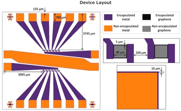
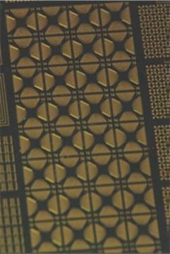
This Graphene FET chip provides 36 graphene devices distributed in a grid pattern on the chip. 30 devices have Hall-bar geometry and 6 have 2-probe geometry.
The Hall-bar devices can be used for Hall measurements as well as 4-probe and 2-probe measurements. There are graphene channels with varied dimensions to allow systematic investigation of device properties.
애플리케이션
특징 및 장점
- State-of-art graphene FETs utilizing consistent high-quality CVD grown monolayer graphene
- Devices are not encapsulated and can be functionalized by additives
- Perfect platform for sensor research and development
- 36 individual graphene FETs per chip
- Mobilities typically > 1000 cm2/V·s
주의사항
To maintain the quality of the devices, we recommend taking the following precautions:
- Be careful when handling the graphene FET chip.
- Tweezers should not contact the device area directly.
Storage Class Code
11 - Combustible Solids
WGK
nwg
Flash Point (°F)
Not applicable
Flash Point (°C)
Not applicable
가장 최신 버전 중 하나를 선택하세요:
이미 열람한 고객
문서
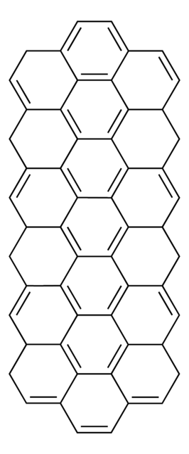
Graphene nanoribbons (GNRs) are quasi-one-dimensional narrow strips of graphene comprised of sp2-hybridized carbon atoms arranged into hexagonal honeycomb lattice configurations.
활성 필터
자사의 과학자팀은 생명 과학, 재료 과학, 화학 합성, 크로마토그래피, 분석 및 기타 많은 영역을 포함한 모든 과학 분야에 경험이 있습니다..
고객지원팀으로 연락바랍니다.