콘텐츠로 건너뛰기
Merck
모든 사진(1)

주요 문서

773697

Sigma-Aldrich

Monolayer graphene film

1 cm x 1 cm on copper foil, avg. no. of layers, 1

로그인조직 및 계약 가격 보기


About This Item

UNSPSC 코드:
12352103
NACRES:
NA.23

양식

film

특징

avg. no. of layers 1

저항성

600 Ω/sq

길이 × 너비 × 두께

1 cm × 1 cm × (theoretical) 0.345 nm, Monolayer graphene film
1.5 cm × 1.5 cm × 25 μm, copper foil substrate

유사한 제품을 찾으십니까? 방문 제품 비교 안내

일반 설명

Catalytic decomposition of hydrocarbons over copper foil forms monolayered graphene films.Graphene deposits as a continuous polycrystalline sheet of individual graphene grains joined at grain boundaries.[1][2]
Graphene film
Growth Method: CVD synthesis
Transfer Method: Clean transfer method
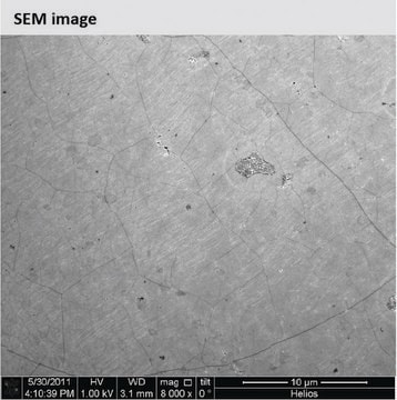
Quality Control: Optical Microscopy & Raman checked
Size: 1 cm x 1 cm
Appearance (Color): Transparent
Transparency: >97%
Appearance (Form): Film
Coverage: >95%
Number of graphene layers: 1
Thickness (theoretical): 0.345 nm
FET Electron Mobility on Al2O3: 2; 000 cm2/V·s
FET Electron Mobility on SiO2/Si (expected): 4; 000 cm2/V·s
Sheet Resistance: 600 Ohms/sq.
Grain size: Up to 10 μm

Substrate Copper Foil
Thickness: 25μm
Both sides: Graphene/Cu/Graphene

Packaging - 4 units/pack

픽토그램

Exclamation mark

신호어

Warning

유해 및 위험 성명서

Hazard Classifications

Eye Irrit. 2 - STOT SE 3

표적 기관

Respiratory system

Storage Class Code

13 - Non Combustible Solids

WGK

WGK 3

Flash Point (°F)

Not applicable

Flash Point (°C)

Not applicable


가장 최신 버전 중 하나를 선택하세요:

시험 성적서(COA)

Lot/Batch Number

적합한 버전을 찾을 수 없으신가요?

특정 버전이 필요한 경우 로트 번호나 배치 번호로 특정 인증서를 찾을 수 있습니다.

이 제품을 이미 가지고 계십니까?

문서 라이브러리에서 최근에 구매한 제품에 대한 문서를 찾아보세요.

문서 라이브러리 방문

이미 열람한 고객

Oleksandr Zagorodko et al.
Analytical chemistry, 86(22), 11211-11216 (2014-10-24)
Strategies employed to interface biomolecules with nanomaterials have considerably advanced in recent years and found practical applications in many different research fields. The construction of nucleic acid modified interfaces together with the label-free detection of hybridization events has been one
Weak mismatch epitaxy and structural feedback in graphene growth on copper foil.
Wilson NR, et al.
Nano Research, 6(2), 99-112 null
Optical nano-imaging of gate-tunable graphene plasmons
Nature (2012)
Xuesong Li et al.
Science (New York, N.Y.), 324(5932), 1312-1314 (2009-05-09)
Graphene has been attracting great interest because of its distinctive band structure and physical properties. Today, graphene is limited to small sizes because it is produced mostly by exfoliating graphite. We grew large-area graphene films of the order of centimeters
Functionalized CVD monolayer graphene for label-free impedimetric biosensing
Eissa S, et al.
Nano Research, 8(5), 1698-1709 null

문서

Fluorescence quenching microscopy visualizes 2D materials like graphene and MoS2 rapidly, inexpensively, and with high fidelity.

Recent demand for electric and hybrid vehicles, coupled with a reduction in prices, has caused lithium-ion batteries (LIBs) to become an increasingly popular form of rechargeable battery technology.

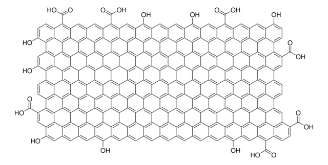
Graphene's unique properties spark interdisciplinary interest; its honeycomb structure offers electrical, optical, and mechanical marvels.

모두 보기

질문

후기

평점 값 없음

활성 필터

자사의 과학자팀은 생명 과학, 재료 과학, 화학 합성, 크로마토그래피, 분석 및 기타 많은 영역을 포함한 모든 과학 분야에 경험이 있습니다..

고객지원팀으로 연락바랍니다.