おすすめの製品
形状
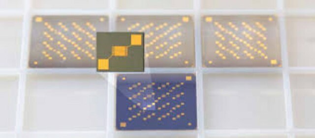
chips (diced)
包装
pack of 1 (wafer of 60 diced chips)
保管温度
15-25°C
類似した製品をお探しですか? 訪問 製品比較ガイド
詳細
Substrate: 150 mm wafer according to semiconductor standard (used for bottom-gate)
Layer structure:
4 x transistors L= 2.5 μm W= 10 mm
4 x transistors L= 5 μm W= 10 mm
4 x transistors L= 10 μm W= 10 mm
4 x transistors L= 20 μm W= 10 mm
Layer structure:
- Gate: n-doped silicon (doping at wafer surface: n~3x10¹⁷/ cm3)
- Gate oxide: 230 nm ± 10 nm SiO2 (thermal oxidation)
- Drain/source: 30 nm Au with 10 nm high work function adhesion layer (ITO), by lift-off technique
- Protection: resist AR PC 5000/3.1 (soluble in AZ-Thinner or acetone)
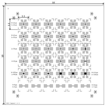
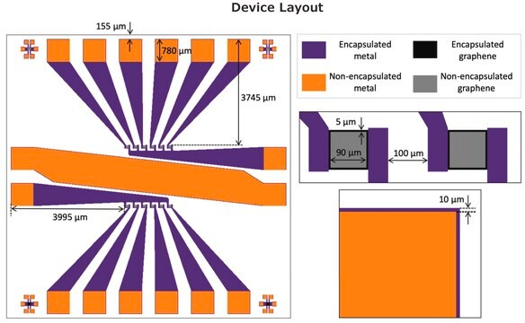
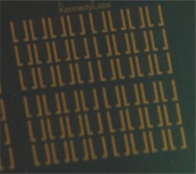
- Layout: see images
- Test chip size: 15 x 15 mm2
- No. of chips: 60 per wafer
- Contact pads: 0.5 x 0.5 mm2
- No. of transistors: 16 per chip
4 x transistors L= 2.5 μm W= 10 mm
4 x transistors L= 5 μm W= 10 mm
4 x transistors L= 10 μm W= 10 mm
4 x transistors L= 20 μm W= 10 mm
アプリケーション
Back-gated OFET Interdigitated Substrate (organic field-effect transistor) can be used in the fabrication of chemical sensors for potential usage in pH sensing and detection of immunoassays. It can also be used in the fabrication of biosensors by coating the sheets of the FET with a specific antibody for the detection of SARS-CoV-2. FET based biosensors can be potentially used in clinical diagnosis, point of care testing, and on-site detection.
包装
diced wafer on foil with air tight packaging
調製ノート
Recommendation for resist removal:
To guarantee a complete cleaning of the wafer / chip surface from resist residuals, please rinse by acetone and then dry the material immediately by nitrogen (compressed air).
Recommendation for material characterization:
If gate currents appear during the characterization of the field effect transistors, considerable variations could occur at the extraction of the carrier mobility. Therefore it is necessary to check the leakage currents over the reverse side (over the chip edges) of the OFET-substrates.
保管および安定性
Store the wafers at a cool and dark place and protect them against sun.
Resist layer was applied to prevent damage from scratches.
Expiration date is the recommended period for resist removal only. After resist removal, the substrate remains functional and does not expire.
Resist layer was applied to prevent damage from scratches.
Expiration date is the recommended period for resist removal only. After resist removal, the substrate remains functional and does not expire.
法的情報
Product of Fraunhofer IPMS
試験成績書(COA)
製品のロット番号・バッチ番号を入力して、試験成績書(COA) を検索できます。ロット番号・バッチ番号は、製品ラベルに「Lot」または「Batch」に続いて記載されています。
Random CNT network and regioregular poly (3-hexylthiophen) FETs for pH sensing applications: A comparison
Munzer AM, et al.
Biochim. Biophys. Acta Gen. Subj., 1830(9), 4353-4358 (2013)
Polymer composite-based OFET sensor with improved sensitivity towards nitro based explosive vapors
Dudhe RS, et al.
Sensors and Actuators B, Chemical, 148(1), 158-165 (2010)
Rapid detection of COVID-19 causative virus (SARS-CoV-2) in human nasopharyngeal swab specimens using field-effect transistor-based biosensor
Seo G, et al.
ACS Nano, 14(4), 5135-5142 (2020)
The impact of biosensing in a pandemic outbreak: COVID-19
Morales-Narvaez E and Dincer C
Biosensors And Bioelectronics, 14(4), 112274-112274 (2020)
資料
Professors Tokito and Takeda share design principles and optimization protocols for organic electronic devices, focusing on flexibility and low cost.
時任教授と竹田教授が、プリントおよび溶液処理された、低コストで高度にフレキシブルな有機エレクトロニクスデバイスのための、新しい材料、デバイス構造設計の原則、および性能最適化のプロトコルを紹介します。
ライフサイエンス、有機合成、材料科学、クロマトグラフィー、分析など、あらゆる分野の研究に経験のあるメンバーがおります。.
製品に関するお問い合わせはこちら(テクニカルサービス)