
GRFETS10

Graphene FET chip
S10
Synonym(s):
Graphene FET, Graphene FET sensor, Graphene FET with 30 Hall-bar devices and 6 2-probe configurations with varied channel geometry
Select a Size
| Size/SKU | Availability | Price |
|---|---|---|
1 ea | Please contact Customer Service for Availability | 2.790,00 PLN |
About This Item
description
Dirac point:< 50 V , Gate Oxide material: SiO2, Gate Oxide thickness: 90 nm, Graphene field-effect mobility: >1000 cm2/V·s, Maximum gate-source voltage: ± 50 V
Maximum temperature rating: 150 °C
Maximum drain-source current density: 107 A/cm2, Metallization: Chromium 2 nm/Gold 50 nm, Monolayer CVD grown Graphene based field effect transistors (FET) S10, Residual charge carrier density: <2 x 1012 cm-2, Resistivity of substrate: 1-10 Ω·cm, Yield >75%
General description
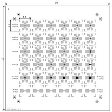
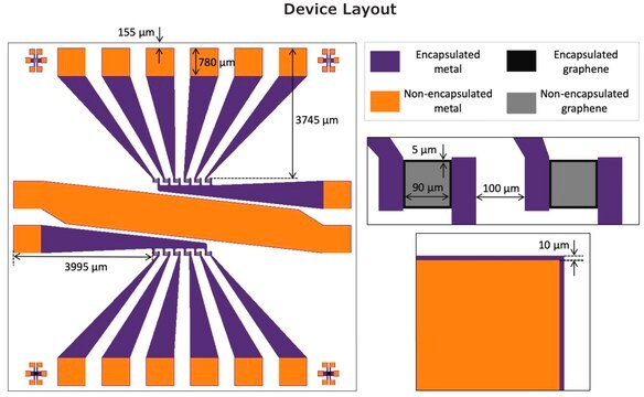
This Graphene FET chip provides 36 graphene devices distributed in a grid pattern on the chip. 30 devices have Hall-bar geometry and 6 have 2-probe geometry.
The Hall-bar devices can be used for Hall measurements as well as 4-probe and 2-probe measurements. There are graphene channels with varied dimensions to allow systematic investigation of device properties.
Application
- Graphene device research
- FET based sensor research for active materials deposited on graphene
- Chemical sensors
- Biosensors
- Bioelectronics
- Magnetic sensors
- Photodetectors
Features and Benefits
- State-of-art graphene FETs utilizing consistent high-quality CVD grown monolayer graphene
- Devices are not encapsulated and can be functionalized by additives
- Perfect platform for sensor research and development
- 36 individual graphene FETs per chip
- Mobilities typically > 1000 cm2/V·s
Disclaimer
To maintain the quality of the devices, we recommend taking the following precautions:
- Be careful when handling the graphene FET chip.
- Tweezers should not contact the device area directly.
1 of 1
This Item | |||
|---|---|---|---|
| description S10 | description S20 | description L × W 1 cm × 1 cm, avg. no. of layers, 1 | description 1 in x 1 in on copper foil, avg. no. of layers, 1 |
| description Yield >75%, Monolayer CVD grown Graphene based field effect transistors (FET) S10, Resistivity of substrate: 1-10 Ω·cm, Gate Oxide material: SiO2, Metallization: Chromium 2 nm/Gold 50 nm | description Monolayer CVD grown Graphene based 2-probe field effect transistors (FET)., Chip dimensions: 10 mm x 10 mm, Resistivity of substrate: 1-10 Ω·cm | description - | description FET Electron Mobility on Al2O3: 2;000 cm2/V·s, Number of graphene layers: 1, FET Electron Mobility on SiO2/Si (expected): 4; 000 cm2/V·s, Grain size: Up to 10 μm, Coverage: >95%, Transparency: >97% |
Still not finding the right product?
Explore all of our products under Graphene FET chip
Storage Class
11 - Combustible Solids
WGK
nwg
Flash Point (°F)
Not applicable
Flash Point (°C)
Not applicable
Choose from one of the most recent versions:
Already Own This Product?
Find documentation for the products that you have recently purchased in the Document Library.