FIPMS176
Back-gated OFET Substrate
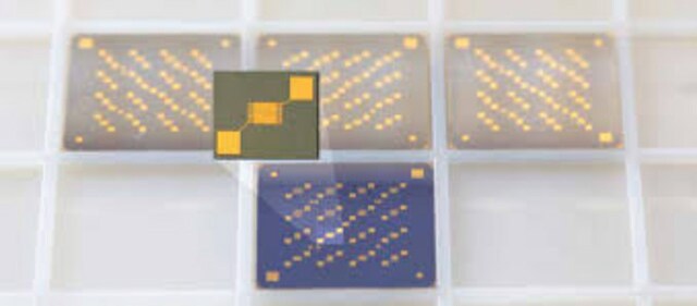
n-doped silicon wafer with 230 nm SiO2 gate-insulator, chips (diced)
Autenticatiper visualizzare i prezzi riservati alla tua organizzazione & contrattuali
About This Item
Codice UNSPSC:
43211915
NACRES:
NA.23
Prodotti consigliati
Forma fisica
chips (diameter 200 mm)
chips (diced)
Confezionamento
pack of 1 (wafer of 112 diced chips)
Descrizione generale
Substrate: 200 mm wafer according to semiconductor standard (used for bottom-gate)
Layer structure:
Layer structure:
- Gate: n-doped silicon (doping at wafer surface: n~3x10¹⁷/ cm3)
- Gate oxide: 230 nm ± 10 nm SiO2 (thermal oxidation)
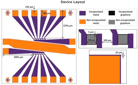
- Drain/source:none
- Protection: resist AR PC 5000/3.1 (soluble in AZ-Thinner or acetone)
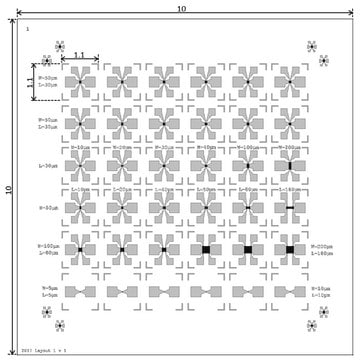
- Layout: bare oxide but diced
- Chip size: 15 x 15 mm2
- No. of chips: 112 per wafer
Applicazioni
Back-gated OFET Substrate (organic field-effect transistor) can be used in the fabrication of chemical sensors for potential usage in pH sensing and detection of immunoassays. It can also be used in the fabrication of biosensors by coating the sheets of the FET with a specific antibody for the detection of SARS-CoV-2. FET based biosensors can be potentially used in clinical diagnosis, point of care testing, and on-site detection.
For material scientists in the field of organic semiconductors, it is critically important to have standardized device architecture for material analysis.
These back-gated organic filed-effect transistor (OFET) substrates were fabricated inside the cleanroom, and source and drain electrodes can be deposited either prior or after the deposition of an organic semiconductor material, giving versatility for the choice of source/drain materials and satisfy different preferred device architectures.
When an organic semiconductor layer is deposited on such a substrate, the bulk Si acts as gate electrode and controls the channel current between the post-deposited source and drain electrodes on the top. A suitably doped Si-SiO2 interface in CMOS quality guarantees a reproducible gate contact.
Confezionamento
diced wafer on foil with air tight packaging
Nota sulla preparazione
Recommendation for resist removal:
To guarantee a complete cleaning of the wafer / chip surface from resist residuals, please rinse by acetone and then dry the material immediately by nitrogen (compressed air).
Recommendation for material characterization:
If gate currents appear during the characterization of the field effect transistors, considerable variations could occur at the extraction of the carrier mobility. Therefore it is necessary to check the leakage currents over the reverse side (over the chip edges) of the OFET-substrates.
Stoccaggio e stabilità
Store the wafers at a cool and dark place and protect them against sun.Resist layer was applied to prevent damage from scratches. Expiration date is the recommended period for resist removal only. After resist removal, the substrate remains functional and does not expire.
Note legali
Product of Fraunhofer IPMS
Certificati d'analisi (COA)
Cerca il Certificati d'analisi (COA) digitando il numero di lotto/batch corrispondente. I numeri di lotto o di batch sono stampati sull'etichetta dei prodotti dopo la parola ‘Lotto’ o ‘Batch’.
Possiedi già questo prodotto?
I documenti relativi ai prodotti acquistati recentemente sono disponibili nell’Archivio dei documenti.
Random CNT network and regioregular poly (3-hexylthiophen) FETs for pH sensing applications: A comparison
Munzer AM, et al.
Biochim. Biophys. Acta Gen. Subj., 1830(9), 4353-4358 (2013)
Polymer composite-based OFET sensor with improved sensitivity towards nitro based explosive vapors
Dudhe RS, et al.
Sensors and Actuators B, Chemical, 148(1), 158-165 (2010)
The impact of biosensing in a pandemic outbreak: COVID-19
Morales-Narvaez E and Dincer C
Biosensors And Bioelectronics, 14(4), 112274-112274 (2020)
Rapid detection of COVID-19 causative virus (SARS-CoV-2) in human nasopharyngeal swab specimens using field-effect transistor-based biosensor
Seo G, et al.
ACS Nano, 14(4), 5135-5142 (2020)
Articoli
Professors Tokito and Takeda share design principles and optimization protocols for organic electronic devices, focusing on flexibility and low cost.
Il team dei nostri ricercatori vanta grande esperienza in tutte le aree della ricerca quali Life Science, scienza dei materiali, sintesi chimica, cromatografia, discipline analitiche, ecc..
Contatta l'Assistenza Tecnica.


