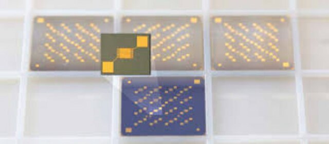
FIPMS267
Back-gated LOFET Circuit Substrate
transistors, inverters and ring oscillators, Ti/TiN source/drain, Au contact, 200 nm gate-insulator, chips (diced)
About This Item
Produits recommandés
Forme
chips (diced)
Conditionnement
pack of 1 (wafer of 56 diced chips)
Température de stockage
15-25°C
Description générale
Structure classes: transistors, inverters, and ring oscillators, additional technology test structures, basic circuits
Die size: 15 × 15 mm2
No. of dies: 56
No. of pads: 39 + 2
Pad size: 1200 × 800 μm2
Gate oxide: 200 nm ± 10 nm
Structured layers: 3 (gate, contacts, source/drain)
Gate layer: Ti/TiN, Rs about 10Ω/sq
Contacts: standard 20 × 20 μm2, R around 20Ω
Top layer: 70 nm Au with 10 nm high work function adhesion layer (ITO), by lift-off technique, Rs about 0.65 Ω/sq/ 0.45 Ω/sq
Documentation: included in shipment
Shadow mask: possible, but not required
Probecard: possible, but not required
Protection: resist protection layer (AR PC 5000/3.1, soluable in AZ-thinner or acetone)
Transistors (11)
Connections:
- shared gate (2 pads on different chip sides)
- shared source (2 pads on different chip sides)
- drain for each transistor
- transfer and output characteristics for each transistor to evaluate new organic semiconductors or to monitor organic material fabrication
- designed for parameter extraction to obtain simulation models
Inverters (4)
All 4 inverters are used within the ring oscillator stages or output drivers
Connections
- shared gate IN for the active transistors (2 pads on different chip sides)
- shared gate GEX for the load transistors (2 pads on different chip sides)
- shared VSS
- VDD and output OUT pads for each inverter
- Layout designed for single transistor separation
- Channel length of all transistors: L=5 μm
- Inverter (input/output) characteristics for rapid monitoring of organic materials
- Supply voltages on VDD and VSS (e.g. for p-type organic material: most positive voltage connected to VDD and ground connected to VSS)
- Voltage on IN (gate of active transistor) with value between VDD and VSS
- Different voltage on GEX (gate of load transistor) changes driver/load ratios
- Important: measure output voltages with high impedance volt meter
Ring oscillators (4)
- Connections - left edge (2 ring oscillators)
- shared gates (GATE_1_2) for all load transistors
- shared VSS
- VDD and output OUT pads for each oscillator
- shared gates (GATE_3_4) for all load transistors
- shared VSS
- VDD and output OUT pads for each oscillator
- 7 or 15 ring stages
- Simple inverter layout or inverter layout, designed for single transistor separation
- Different driver/load ratios
- Channel length of all transistors: L=5 μm
- Measure result: oscillation frequency on OUT and calculated inverter delay
- No input signal required
- Supply voltages on VDD and VSS (e.g. for p-type organic material: most positive voltage connected to VDD and ground connected to VSS)
- Different voltage on GEX (gate of load transistors) changes driver/load ratios
- Changing these voltage (more positive or more negative than VSS) triggers oscillation
- Measure output: high impedance oscilloscope probe required
Application
Conditionnement
Notes préparatoires
To guarantee a complete cleaning of the wafer / chip surface from resist residuals, please rinse by acetone and then dry the material immediately by nitrogen (compressed air).
Recommendation for material characterization:
If gate currents appear during the characterization of the field effect transistors, considerable variations could occur at the extraction of the carrier mobility. Therefore it is necessary to check the leakage currents over the reverse side (over the chip edges) of the OFET-substrates.
Stockage et stabilité
Resist layer was applied to prevent damage from scratches.
Expiration date is the recommended period for resist removal only. After resist removal, the substrate remains functional and does not expire.
Informations légales
Faites votre choix parmi les versions les plus récentes :
Certificats d'analyse (COA)
Désolés, nous n'avons pas de COA pour ce produit disponible en ligne pour le moment.
Si vous avez besoin d'assistance, veuillez contacter Service Clients
Déjà en possession de ce produit ?
Retrouvez la documentation relative aux produits que vous avez récemment achetés dans la Bibliothèque de documents.
Articles
Professors Tokito and Takeda share design principles and optimization protocols for organic electronic devices, focusing on flexibility and low cost.
Notre équipe de scientifiques dispose d'une expérience dans tous les secteurs de la recherche, notamment en sciences de la vie, science des matériaux, synthèse chimique, chromatographie, analyse et dans de nombreux autres domaines..
Contacter notre Service technique


