900415
Graphene, monolayer film
10 cm x 10 cm on copper foil, avg. no. of layers, 1
Synonym(s):
Graphene/Cu
About This Item
Recommended Products
Product Name
Monolayer graphene film, 10 cm x 10 cm on copper foil, avg. no. of layers, 1
Quality Level
form
film
feature
avg. no. of layers 1
Looking for similar products? Visit Product Comparison Guide
General description
- Graphene film.
- Growth method: CVD synthesis.
- Appearance: Transparent film.
- Transparency: >97%.
- Coverage: >95%.
- Number of graphene layers: 1.
- Thickness (theoretical): 0.345 nm.
- FET electron mobility on Al2O3: 2000 cm2/Vs.
- Hall electron mobility on SiO2/Si: 4000 cm2/Vs.
- Sheet resistance on SiO2/Si: 450±40 Ω/sq (1cm x1cm).
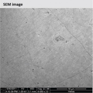
- Grain size: Up to 10 μm.
- Substrate: Copper Foil.
- Thickness: 18 μm.
Application
- Flexible batteries.
- Electronics.
- Aerospace industry.
- MEMS and NEMS.
- Microactuators.
- Conductive coatings.
Storage Class Code
13 - Non Combustible Solids
WGK
WGK 2
Flash Point(F)
Not applicable
Flash Point(C)
Not applicable
Choose from one of the most recent versions:
Already Own This Product?
Find documentation for the products that you have recently purchased in the Document Library.
Customers Also Viewed
Articles
Professors summarize recent 2D materials synthesis advancements and biosensing applications in various fields.
Professors summarize recent 2D materials synthesis advancements and biosensing applications in various fields.
Professors summarize recent 2D materials synthesis advancements and biosensing applications in various fields.
Professors summarize recent 2D materials synthesis advancements and biosensing applications in various fields.
Our team of scientists has experience in all areas of research including Life Science, Material Science, Chemical Synthesis, Chromatography, Analytical and many others.
Contact Technical Service


