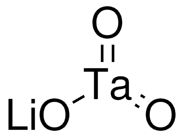
254290
Lithium niobate
99.9% trace metals basis
Synonym(s):
Lithium metaniobatem, Lithium niobium oxide, Lithium niobium trioxide
Sign Into View Organizational & Contract Pricing
All Photos(2)
About This Item
Linear Formula:
LiNbO3
CAS Number:
Molecular Weight:
147.85
EC Number:
MDL number:
UNSPSC Code:
12161600
PubChem Substance ID:
NACRES:
NA.22
Recommended Products
Quality Level
Assay
99.9% trace metals basis
form
powder
reaction suitability
core: niobium
reagent type: catalyst
particle size
200 mesh
SMILES string
[Li+].[O-][Nb](=O)=O
InChI
1S/Li.Nb.3O/q+1;;;;-1
InChI key
GQYHUHYESMUTHG-UHFFFAOYSA-N
Storage Class Code
11 - Combustible Solids
WGK
WGK 3
Flash Point(F)
Not applicable
Flash Point(C)
Not applicable
Choose from one of the most recent versions:
Already Own This Product?
Find documentation for the products that you have recently purchased in the Document Library.
Customers Also Viewed
Julien Macario et al.
Optics express, 20(21), 23623-23629 (2012-11-29)
In recent years, the development of new lithium niobate electro-optic modulator designs and material processing techniques have contributed to support the increasing need for faster optical networks by considerably extending the operational bandwidth of modulators. In an effort to provide
Jesper B Christensen et al.
Molecules (Basel, Switzerland), 26(3) (2021-01-29)
We report on the use of quartz-enhanced photoacoustic spectroscopy for continuous carbon-dioxide measurements in humid air over a period of six days. The presence of water molecules alters the relaxation rate of the target molecules and thus the amplitude of
An all-optical technique enables instantaneous single-shot demodulation of images at high frequency.
Swapnesh Panigrahi et al.
Nature communications, 11(1), 549-549 (2020-01-30)
High-frequency demodulation of wide area optical signals in a snapshot manner remains a technological challenge. If solved, it could open tremendous perspectives in 3D imaging, vibrometry, free-space communications, automated vision, or ballistic photon imaging in scattering media with numerous applications
Lisa Miccio et al.
Lab on a chip, 12(21), 4449-4454 (2012-09-11)
We explore a novel approach for fabricating polymeric microfluidic-channelled dielectrophoretic (DEP) chips by direct laser projection through a holographic Spatial-Light-Modulator (SLM) onto photorefractive crystal substrates. As the first step, an all-optical mould-free approach was used to fabricate the PDMS microfluidic
Haidong Lu et al.
Advanced materials (Deerfield Beach, Fla.), 31(48), e1902890-e1902890 (2019-10-08)
Domain wall nanoelectronics is a rapidly evolving field, which explores the diverse electronic properties of the ferroelectric domain walls for application in low-dimensional electronic systems. One of the most prominent features of the ferroelectric domain walls is their electrical conductivity.
Our team of scientists has experience in all areas of research including Life Science, Material Science, Chemical Synthesis, Chromatography, Analytical and many others.
Contact Technical Service


