
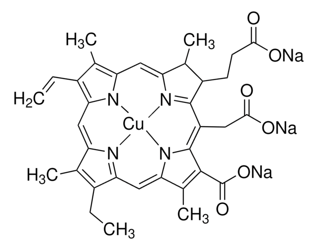
329010
Gallium arsenide
pieces, 99.999% trace metals basis
Sign Into View Organizational & Contract Pricing
All Photos(1)
About This Item
Linear Formula:
GaAs
CAS Number:
Molecular Weight:
144.64
EC Number:
MDL number:
UNSPSC Code:
12352300
PubChem Substance ID:
Recommended Products


Assay
99.999% trace metals basis
form
pieces
density
5.31 g/mL at 25 °C (lit.)
SMILES string
[Ga]#[As]
InChI
1S/As.Ga
InChI key
JBRZTFJDHDCESZ-UHFFFAOYSA-N
Looking for similar products? Visit Product Comparison Guide

Signal Word
Danger
Hazard Statements
Precautionary Statements
Hazard Classifications
Carc. 1B - Repr. 1B - STOT RE 1
Target Organs
Respiratory system,hematopoietic system
Storage Class Code
6.1A - Combustible acute toxic Cat. 1 and 2 / very toxic hazardous materials
WGK
WGK 3
Flash Point(F)
Not applicable
Flash Point(C)
Not applicable
Choose from one of the most recent versions:
Already Own This Product?
Find documentation for the products that you have recently purchased in the Document Library.
Yu Bomze et al.
Physical review letters, 109(2), 026801-026801 (2012-10-04)
We report on measurements of first-passage-time distributions associated with current switching in weakly coupled GaAs/AlAs superlattices driven by shot noise, a system that is both far from equilibrium and high dimensional. Static current-voltage (I-V) characteristics exhibit multiple current branches and
Chan Il Yeo et al.
Optics express, 20(17), 19554-19562 (2012-10-06)
We present a simple, cost-effective, large scale fabrication technique for antireflective disordered subwavelength structures (d-SWSs) on GaAs substrate by Ag etch masks formed using spin-coated Ag ink and subsequent inductively coupled plasma (ICP) etching process. The antireflection characteristics of GaAs
Shih-Wei Tan et al.
PloS one, 7(11), e50681-e50681 (2012-12-12)
Characterization and modeling of metal-semiconductor-metal (MSM) GaAs diodes using to evaporate SiO₂ and Pd simultaneously as a mixture electrode (called M-MSM diodes) compared with similar to evaporate Pd as the electrode (called Pd-MSM diodes) were reported. The barrier height (φ(b))
Chao-Wei Hsu et al.
Nanotechnology, 23(49), 495306-495306 (2012-11-17)
GaAs is grown by metal-organic vapor-phase epitaxy on a 55 nm round-hole patterned Si substrate with SiO(2) as a mask. The threading dislocations, which are stacked on the lowest energy facet plane, move along the SiO(2) walls, reducing the number
[A matrix gallium-arsenide detector for roentgenoraphy].
A P Vorob'ev et al.
Meditsinskaia tekhnika, (5)(5), 21-26 (2012-11-20)
Active Filters
Our team of scientists has experience in all areas of research including Life Science, Material Science, Chemical Synthesis, Chromatography, Analytical and many others.
Contact Technical Service