GRFETS10
Graphene FET chip
S10
Synonym(s):
Graphene FET, Graphene FET sensor, Graphene FET with 30 Hall-bar devices and 6 2-probe configurations with varied channel geometry
About This Item
Recommended Products
description
Dirac point:< 50 V
Gate Oxide material: SiO2
Gate Oxide thickness: 90 nm
Graphene field-effect mobility: >1000 cm2/V·s
Maximum gate-source voltage: ± 50 V
Maximum temperature rating: 150 °C
Maximum drain-source current density: 107 A/cm2
Metallization: Chromium 2 nm/Gold 50 nm
Monolayer CVD grown Graphene based field effect transistors (FET) S10
Residual charge carrier density: <2 x 1012 cm-2
Resistivity of substrate: 1-10 Ω·cm
Yield >75%
Looking for similar products? Visit Product Comparison Guide
General description
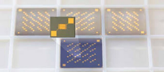
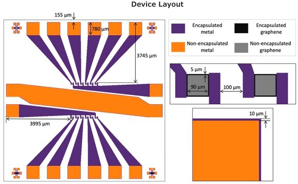
This Graphene FET chip provides 36 graphene devices distributed in a grid pattern on the chip. 30 devices have Hall-bar geometry and 6 have 2-probe geometry.
The Hall-bar devices can be used for Hall measurements as well as 4-probe and 2-probe measurements. There are graphene channels with varied dimensions to allow systematic investigation of device properties.
Application
- Graphene device research
- FET based sensor research for active materials deposited on graphene
- Chemical sensors
- Biosensors
- Bioelectronics
- Magnetic sensors
- Photodetectors
Features and Benefits
- State-of-art graphene FETs utilizing consistent high-quality CVD grown monolayer graphene
- Devices are not encapsulated and can be functionalized by additives
- Perfect platform for sensor research and development
- 36 individual graphene FETs per chip
- Mobilities typically > 1000 cm2/V·s
Caution
To maintain the quality of the devices, we recommend taking the following precautions:
- Be careful when handling the graphene FET chip.
- Tweezers should not contact the device area directly.
Storage Class Code
11 - Combustible Solids
WGK
nwg
Flash Point(F)
Not applicable
Flash Point(C)
Not applicable
Certificates of Analysis (COA)
Search for Certificates of Analysis (COA) by entering the products Lot/Batch Number. Lot and Batch Numbers can be found on a product’s label following the words ‘Lot’ or ‘Batch’.
Already Own This Product?
Find documentation for the products that you have recently purchased in the Document Library.
Customers Also Viewed
Articles
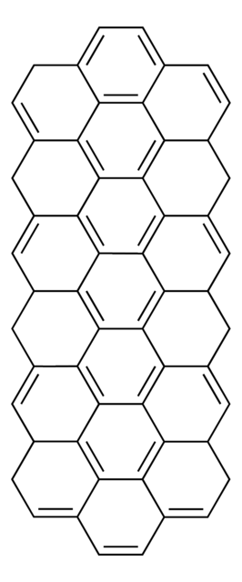
Graphene nanoribbons (GNRs) are quasi-one-dimensional narrow strips of graphene comprised of sp2-hybridized carbon atoms arranged into hexagonal honeycomb lattice configurations.
Graphene nanoribbons (GNRs) are quasi-one-dimensional narrow strips of graphene comprised of sp2-hybridized carbon atoms arranged into hexagonal honeycomb lattice configurations.
Graphene nanoribbons (GNRs) are quasi-one-dimensional narrow strips of graphene comprised of sp2-hybridized carbon atoms arranged into hexagonal honeycomb lattice configurations.
Graphene nanoribbons (GNRs) are quasi-one-dimensional narrow strips of graphene comprised of sp2-hybridized carbon atoms arranged into hexagonal honeycomb lattice configurations.
Our team of scientists has experience in all areas of research including Life Science, Material Science, Chemical Synthesis, Chromatography, Analytical and many others.
Contact Technical Service