
649805
PEDOT, block PEG
solution, 1 wt. % dispersion in nitromethane, contains perchlorate as dopant
Sinónimos:
Aedotron™ C-NM
About This Item
Productos recomendados


Nombre del producto
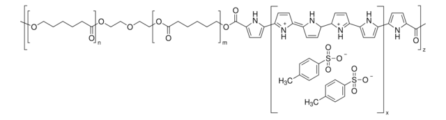
Poly(3,4-ethylenedioxythiophene)-block-poly(ethylene glycol) solution, 1 wt % dispersion in nitromethane, contains perchlorate as dopant
contiene
perchlorate as dopant
Nivel de calidad
concentración
1 wt % dispersion in nitromethane
resistencia
10,000-100,000 Ω/sq (spin cast thin films: typically 1-3 layers spun at 1,000 rpm)
función de trabajo
4.33 eV
descripción
40 nm (RMS roughness spin cast thin films)
tamaño de partícula
600-1000 nm (in suspension)
conductividad
0.1-5.0 S/cm (bulk)
densidad
1.127 g/mL at 25 °C
¿Está buscando productos similares? Visita Guía de comparación de productos
Descripción general
Aplicación
Precaución
Información legal


Palabra de señalización
Warning
Frases de peligro
Consejos de prudencia
Clasificaciones de peligro
Acute Tox. 4 Inhalation - Acute Tox. 4 Oral - Carc. 2 - Flam. Liq. 3 - Repr. 2
Código de clase de almacenamiento
3 - Flammable liquids
Clase de riesgo para el agua (WGK)
WGK 2
Punto de inflamabilidad (°F)
96.8 °F - closed cup
Punto de inflamabilidad (°C)
36 °C - closed cup
Elija entre una de las versiones más recientes:
¿Ya tiene este producto?
Encuentre la documentación para los productos que ha comprado recientemente en la Biblioteca de documentos.
Los clientes también vieron

Artículos
In the field of organic printable electronics, such as OLEDs and organic photovoltaics (OPVs), improved organic conducting and semiconducting materials are needed. The progress in two fields is reviewed in this article.
In the field of organic printable electronics, such as OLEDs and organic photovoltaics (OPVs), improved organic conducting and semiconducting materials are needed. The progress in two fields is reviewed in this article.
In the field of organic printable electronics, such as OLEDs and organic photovoltaics (OPVs), improved organic conducting and semiconducting materials are needed. The progress in two fields is reviewed in this article.
In the field of organic printable electronics, such as OLEDs and organic photovoltaics (OPVs), improved organic conducting and semiconducting materials are needed. The progress in two fields is reviewed in this article.
Nuestro equipo de científicos tiene experiencia en todas las áreas de investigación: Ciencias de la vida, Ciencia de los materiales, Síntesis química, Cromatografía, Analítica y muchas otras.
Póngase en contacto con el Servicio técnico