FIPMS176
Back-gated OFET Substrate
n-doped silicon wafer with 230 nm SiO2 gate-insulator, chips (diced)
About This Item
Produits recommandés
Forme
chips (diameter 200 mm)
chips (diced)
Conditionnement
pack of 1 (wafer of 112 diced chips)
Description générale
Layer structure:
- Gate: n-doped silicon (doping at wafer surface: n~3x10¹⁷/ cm3)
- Gate oxide: 230 nm ± 10 nm SiO2 (thermal oxidation)
- Drain/source:none
- Protection: resist AR PC 5000/3.1 (soluble in AZ-Thinner or acetone)
- Layout: bare oxide but diced
- Chip size: 15 x 15 mm2
- No. of chips: 112 per wafer
Application
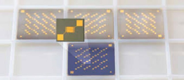
These back-gated organic filed-effect transistor (OFET) substrates were fabricated inside the cleanroom, and source and drain electrodes can be deposited either prior or after the deposition of an organic semiconductor material, giving versatility for the choice of source/drain materials and satisfy different preferred device architectures.
When an organic semiconductor layer is deposited on such a substrate, the bulk Si acts as gate electrode and controls the channel current between the post-deposited source and drain electrodes on the top. A suitably doped Si-SiO2 interface in CMOS quality guarantees a reproducible gate contact.
Conditionnement
Notes préparatoires
To guarantee a complete cleaning of the wafer / chip surface from resist residuals, please rinse by acetone and then dry the material immediately by nitrogen (compressed air).
Recommendation for material characterization:
If gate currents appear during the characterization of the field effect transistors, considerable variations could occur at the extraction of the carrier mobility. Therefore it is necessary to check the leakage currents over the reverse side (over the chip edges) of the OFET-substrates.
Stockage et stabilité
Informations légales
Certificats d'analyse (COA)
Recherchez un Certificats d'analyse (COA) en saisissant le numéro de lot du produit. Les numéros de lot figurent sur l'étiquette du produit après les mots "Lot" ou "Batch".
Déjà en possession de ce produit ?
Retrouvez la documentation relative aux produits que vous avez récemment achetés dans la Bibliothèque de documents.
Articles
Professors Tokito and Takeda share design principles and optimization protocols for organic electronic devices, focusing on flexibility and low cost.
Professors Tokito and Takeda share design principles and optimization protocols for organic electronic devices, focusing on flexibility and low cost.
Professors Tokito and Takeda share design principles and optimization protocols for organic electronic devices, focusing on flexibility and low cost.
Professors Tokito and Takeda share design principles and optimization protocols for organic electronic devices, focusing on flexibility and low cost.
Notre équipe de scientifiques dispose d'une expérience dans tous les secteurs de la recherche, notamment en sciences de la vie, science des matériaux, synthèse chimique, chromatographie, analyse et dans de nombreux autres domaines..
Contacter notre Service technique


