798177
Graphene, monolayer film
on TEM grid substrate (Quantifoil gold)
Sign Into View Organizational & Contract Pricing
All Photos(1)
About This Item
Linear Formula:
C
UNSPSC Code:
12352103
NACRES:
NA.23
Recommended Products
Product Name
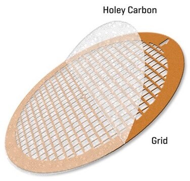
Suspended monolayer graphene on TEM grid substrate (Quantifoil gold),
form
solid
Quality Level
resistance
170 Ω/sq
diam. × thickness
2 mm × (theoretical) 0.345 nm , monolayer graphene film
size × distance between discs × diam.
2 μm × 4 μm × 3 mm, gold coated TEM grid
Related Categories
General description
Graphene is a unique one-atom thick, two dimensional allotrope of carbon. Several methods have been developed to synthesize graphene, such as; mechanical and chemical exfoliation, chemical vapor deposition, graphitization of silicon carbide, reduction of graphene oxides. Preparation of monolayer graphene on polyethylene terephthalate (PET) film has been reported in a study. The single layer of graphene can be transferred by clean transfer method.
Grids per package:4
Graphene Film Properties
Growth Method: CVD synthesis
Transfer Method: Clean transfer method
Size: 2 mm (TEM grid diameter)
Appearance (Color): Transparent
Transparency: >97%
Coverage: >95%
Number of graphene layers: single layer
Thickness of the lazy carbon is about 12 nm.
FET Electron Mobility on Al2O3: 2; 000 cm2/Vs
FET Electron Mobility on SiO2/Si (expected): 4; 000 cm2/Vs
Sheet Resistance: 170 Ohms/sq.
Grain size: up to 10 micrometer
Substrate TEM grid
Type: QUANTIFOIL(registered) R 2/4
Hole Size: 2 micrometers(Au grid is 300 mesh)
Space between holes: 4 micrometers
Diameter: 3 mm
Coating: Au coated
Application
Graphene film on TEM grid is useful for high resolution TEM imaging of nanoscale materials because it preserves the same focal plane over the whole grid mesh.
Storage Class Code
11 - Combustible Solids
WGK
WGK 3
Flash Point(F)
Not applicable
Flash Point(C)
Not applicable
Choose from one of the most recent versions:
Already Own This Product?
Find documentation for the products that you have recently purchased in the Document Library.
Customers Also Viewed
Progress of graphene growth on copper by chemical vapor deposition: Growth behavior and controlled synthesis
LeiPeng MA,et al.
Chinese Science Bulletin, 57(23), 2995-2999 null
Nanopores: Graphene opens up to DNA.
Zuzanna S Siwy et al.
Nature nanotechnology, 5(10), 697-698 (2010-10-07)
Stanislav M Avdoshenko et al.
Nano letters, 13(5), 1969-1976 (2013-04-17)
Graphene layers have been targeted in the last years as excellent host materials for sensing a remarkable variety of gases and molecules. Such sensing abilities can also benefit other important scientific fields such as medicine and biology. This has automatically
Controlled Synthesis of Monolayer Graphene Toward Transparent Flexible Conductive Film Application
Jee BJ, et al.
Nanoscale Research Letters, 5, 1768?1773-1768?1773 (2010)
Our team of scientists has experience in all areas of research including Life Science, Material Science, Chemical Synthesis, Chromatography, Analytical and many others.
Contact Technical Service