GRFETS10
Graphene FET chip
S10
Sinónimos:
Graphene FET, Graphene FET sensor, Graphene FET with 30 Hall-bar devices and 6 2-probe configurations with varied channel geometry
About This Item
Productos recomendados
description
Dirac point:< 50 V
Gate Oxide material: SiO2
Gate Oxide thickness: 90 nm
Graphene field-effect mobility: >1000 cm2/V·s
Maximum gate-source voltage: ± 50 V
Maximum temperature rating: 150 °C
Maximum drain-source current density: 107 A/cm2
Metallization: Chromium 2 nm/Gold 50 nm
Monolayer CVD grown Graphene based field effect transistors (FET) S10
Residual charge carrier density: <2 x 1012 cm-2
Resistivity of substrate: 1-10 Ω·cm
Yield >75%
¿Está buscando productos similares? Visita Guía de comparación de productos
General description
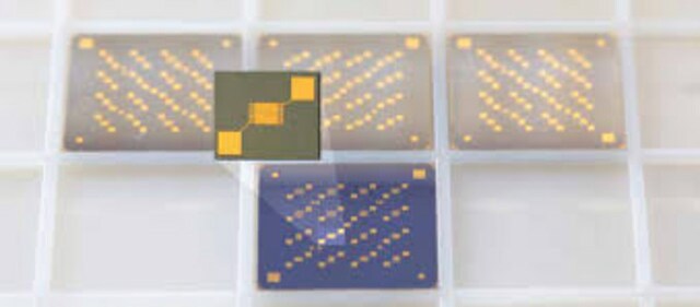
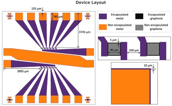
This Graphene FET chip provides 36 graphene devices distributed in a grid pattern on the chip. 30 devices have Hall-bar geometry and 6 have 2-probe geometry.
The Hall-bar devices can be used for Hall measurements as well as 4-probe and 2-probe measurements. There are graphene channels with varied dimensions to allow systematic investigation of device properties.
Application
- Graphene device research
- FET based sensor research for active materials deposited on graphene
- Chemical sensors
- Biosensors
- Bioelectronics
- Magnetic sensors
- Photodetectors
Features and Benefits
- State-of-art graphene FETs utilizing consistent high-quality CVD grown monolayer graphene
- Devices are not encapsulated and can be functionalized by additives
- Perfect platform for sensor research and development
- 36 individual graphene FETs per chip
- Mobilities typically > 1000 cm2/V·s
Caution
To maintain the quality of the devices, we recommend taking the following precautions:
- Be careful when handling the graphene FET chip.
- Tweezers should not contact the device area directly.
Storage Class
11 - Combustible Solids
wgk_germany
nwg
flash_point_f
Not applicable
flash_point_c
Not applicable
Certificados de análisis (COA)
Busque Certificados de análisis (COA) introduciendo el número de lote del producto. Los números de lote se encuentran en la etiqueta del producto después de las palabras «Lot» o «Batch»
¿Ya tiene este producto?
Encuentre la documentación para los productos que ha comprado recientemente en la Biblioteca de documentos.
Los clientes también vieron
Artículos
Graphene nanoribbons (GNRs) are quasi-one-dimensional narrow strips of graphene comprised of sp2-hybridized carbon atoms arranged into hexagonal honeycomb lattice configurations.
Graphene nanoribbons (GNRs) are quasi-one-dimensional narrow strips of graphene comprised of sp2-hybridized carbon atoms arranged into hexagonal honeycomb lattice configurations.
Graphene nanoribbons (GNRs) are quasi-one-dimensional narrow strips of graphene comprised of sp2-hybridized carbon atoms arranged into hexagonal honeycomb lattice configurations.
Graphene nanoribbons (GNRs) are quasi-one-dimensional narrow strips of graphene comprised of sp2-hybridized carbon atoms arranged into hexagonal honeycomb lattice configurations.
Nuestro equipo de científicos tiene experiencia en todas las áreas de investigación: Ciencias de la vida, Ciencia de los materiales, Síntesis química, Cromatografía, Analítica y muchas otras.
Póngase en contacto con el Servicio técnico