Polytriarylamine Semiconductors
Iain McCulloch, Martin Heeney
Flexink Limited - Southampton, UK
Material Matters 2009, 4.3, 70.
Application of Solution Processable Organic Semiconductors in Organic Electronics
Organic electronics is an emerging scientific field of potentially huge technological and commercial relevance1, and is an increasingly ubiquitous research activity globally. One important area is the development of organic field effect transistors (OFET) which can potentially be employed in applications such as RFID tags and display backplanes.2,3 In order to be commercially competitive, these devices must be printed by a low-cost, high throughput process. Additive solution based printing techniques such as ink-jet and contact printing are considered to be attractive processing options. In order to satisfy these printing requirements, the semiconductor material should be formulated into an ink, with appropriate rhelology. There are several potentially high performing semiconductors that have been disclosed in the literature recently that can be deposited from solution into thin films.4-7 In almost all cases, however, aggressive and environmentally unfriendly solvents are required to fully dissolve these crystalline polymers, without which potentially difficult suspensions or gels can form.8 Additionally, the device fabrication process typically requires a pre-treatment step to reduce the energy of the coating surface, as well as a thermal annealing step after semiconductor deposition to induce optimal crystallinity.9 Both these additional steps potentially add cost to the process. Another drawback with some thiophene based polymers is that the high electron density over extended conjugation lengths leads to high lying HOMO energy levels with corresponding susceptibility to electrochemical oxidation in ambient conditions. Even in situations where acceptable ambient stability is demonstrated in storage conditions, devices that are driven at high current density conditions or where a bottom-gate transistor architecture is employed, where the semiconductor film is the exposed surface, suffer from instabilities. These instabilities manifest as a deterioration in the large initial carrier mobilities to significantly lower values over short periods.10 Clearly then, there is a demand for fully air stable polymers that can be easily deposited from environmentally friendly solvents, do not require further treatment to obtain optimal performance and have the flexibility to be employed in any device architecture. Polytriarylamines fit these requirements: they are highly soluble, amorphous semiconducting polymers11 which require no annealing and can achieve stable charge carrier mobilities of the order of 5 x 10⁻³ cm2/Vs in both top and bottom gate transistor architectures.12 The presence of the amine nitrogen in the polymer backbone acts to prevent efficient delocalization of π electrons between adjacent phenyl units, thus limiting the effective conjugation length and resulting in low lying HOMO energy levels and excellent oxidative stability. The non-planar, rotationally-free and large linkage angle backbone however prevents optimal intermolecular π-electron aromatic stacking, leading to an amorphous microstructure and limiting the charge carrier mobility to lower values than some highly ordered crystalline materials. However, this ease of processing and robust electrical performance offers significant compensation.
Synthesis
Poly(bis(4-phenyl)(2,4,6-trimethylphenyl)amine) (Prod. No. 702471) was synthesised by palladium catalysed Suzuki coupling, as shown in Figure 1. To eliminate the effects of unbalanced stoichiometry, a homo-condensation reaction was employed with the asymmetrically bifunctionalized bromo boronate of the triarylamine repeat unit. Purification of the crude polymer is essential, affording the polymer as yellow solid, soluble in common organic solvents such as tolulene (Prod. No. 568821), chloroform (Prod. No. 372978) and xylene (Prod. No. 296333). Number average molecular weights of over 45 Kda can be obtained by this procedure, with polydispersities of between 2 and 3.

Figure 1. Synthesis of Poly(bis(4-phenyl)(2,4,6-trimethylphenyl)amine) by palladium catalyzed Suzuki coupling.
Transistor Devices
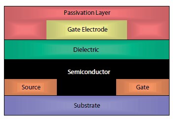
Field effect transistor devices were fabricated on a glass substrate (Corning® EAGLE 2000) using a bottom-contact, top-gate architecture, often referred to as a staggered geometry, as shown in Figure 2. The glass was cleaned by sonication in a detergent solution. Source and drain electrodes were evaporated Au treated with a pentafluorobenzenethiol (PFBT) self-assembled monolayer. Typical channel dimensions were 30 μM length and 1000 μM width. Polymers were spin coated from a 10 mg/ml solution in chlorobenzene at 2000 rpm and dried at 100 °C for 2 min. The gate dielectric was a fluoropolymer CYTOP and again deposited by spin coating from a 9 wt% solution in FC43 solvent, and dried at 100 °C. Top-gate electrodes were evaporated aluminum. Device fabrication was carried out under nitrogen with storage and electrical testing in air for the stability tests.

Figure 2. Top gate, staggered contact transistor architecture
Transistors were characterised using a Keithley 4200 semiconductor parameter analyzer. Saturation mobilities were calculated using a standard thin film transistor model according to the equation below:

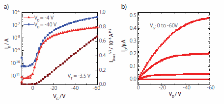
where Ci is the geometric capacitance of the gate dielectric (2.1 nFcm-2). Carrier mobilities of 5x10⁻³ cm2/Vs were extracted from the currentvoltage characteristics shown in Figure 3. The transfer characteristics of a typical device is shown in Figure 3(a), with ON/OFF ratios of about 104 and a threshold voltage close to 0 V. As illustrated in the linear shape of output characteristics at low source drain voltage (Figure 3(b)) the PFBT electrode treatment successfully lowers the Au work function, thus ensuring that there are no contact injection problems.

Figure 3. Transfer (a) and output (b) characteristics of a PTAA top-gate bottomcontact device with Cytop dielectric and Au source and drain electrodes treated with pentafluorobenzenethiol. Channel length (L) was 30 microns and width (W) was 1000 microns corresponding to a charge carrier mobility of 5 x 10⁻³ cm2/Vs.
Conclusion
Polyarylamines are a versatile class of air stable, solution processable organic semiconductors. Their performance has been shown to be inert to ambient air and humidity, which for long term operation provides sustained and consistent currents, outperforming most of the less stable semiconductors. Their amorphous nature contributes to high solubility in a range of formulation solvents, with many choices outside the typical chlorinated aromatic solvents necessary for dissolution of highly crystalline thiophene containing polymers. Neither surface alignment layers, or high temperature annealing are required to obtain optimal performance, illustrating the flexible nature of these polymers.
References
To continue reading please sign in or create an account.
Don't Have An Account?