Self-Assembly in Organic Thin Film Transistors for Flexible Electronic Devices
Zhenan Bao
Material Matters 2006, 1.2, 11.
Introduction
Flexible electronic circuits and displays based on organic active materials are future generations of products that may eventually enter mainstream electronics market. The advantages in using organic active materials are their ease in tuning electronic and processing properties by chemical design and synthesis, low cost processing based on low temperature processes and reel-to-reel printing methods, mechanical flexibility, and compatibility with flexible substrates.1
Organic thin film transistors (OTFTs) are the basic building blocks for flexible integrated circuits and displays. A schematic structure is shown in Figure 1.2

Figure 1.Schematic structure of an organic thin film transistor. (a) Chemical structure of the silane molecule used as the self-assembled monolayer dielectric layer (b) Chemical structure of pentacene used as the semiconductor layer (c ) schematic structure of the device. Reproduced with permission from the Nature Publishing Group.
During the operation of the transistor, a gate electrode is used to control the current flow between the drain and source electrodes. Typically, a higher applied gate voltage leads to higher current flow between drain and source electrodes. A fast switching transistor should have a high charge carrier mobility and a high on/off current ratio for the semiconductor material. For the pixel switching transistors in liquid crystal displays, mobility greater than 0.1 cm2/Vs and on/off ratio greater than 106 are needed.
Both self-assemblies and self-assembly processes play important roles in improving device performance as well as enabling low cost processing methods for the fabrication of these devices. In this article, a briefly survey is given on the applications of self-assembly in OTFTs.
Surface modification with self-assembled monolayers (SAMs)
Drain and source electrode surface modification with SAMs
For organic transistors to function well, charge injection from the electrode needs to be efficient. This requires the work function of the electrode to match well with the energy level of the organic semiconductor such that the energy barrier for charge injection is low. For organic transistors, typically high work function electrodes (Au, Pd, or indium tin oxide) have been used for p-channel organic semiconductors, in which holes are injected and transported through the organic material. It has been found that electrode surface modification with a self-assembled monolayer can be used to improve the charge injection into the organic semiconductor.3 For example, when Au electrodes are used, they can be functionalized with various thiol SAMs to tune their work functions. Moreover, the morphology of organic semiconductors is significantly different when deposited on SAM modified Au compared to bare Au. This observation has been used to tune the morphology of the organic semiconductor at the Au/organic interface to improve its charge injection.4
Dielectric surface modification
Surface treatment of dielectric layer is an important way to improve organic transistor performance. Since most of the charge carriers induced in the semiconductor layer are confined to the first 5 nm of organic semiconductor from the semiconductor/dielectric interface, the dielectric surface chemical and physical characteristics thus play a significant role on the charge carrier transport. For example, Si-OH groups on SiO2 surface (a typical dielectric material) is known to trap electrons. Capping SiO2 surfaces with octadecyl trichlorosilane (OTS) molecules can significantly reduce electron traps and improve mobility of n-channel semiconductors (electrons are the major charge carriers).5
Additionally, dielectric surface treatment with SAMs also affects the nucleation and growth of organic semiconductors.6 For example, pentacene is an organic semiconductor with the highest reported thin film charge carrier mobility. Its charge carrier mobility changes significantly depending on the types of hydrophobic SAM surface treatment. This difference is related to the morphological difference of the first pentacene monolayer formed on different surfaces.6
SAMs as the active dielectric or semiconductor layers
Dielectric layer
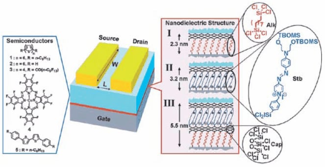
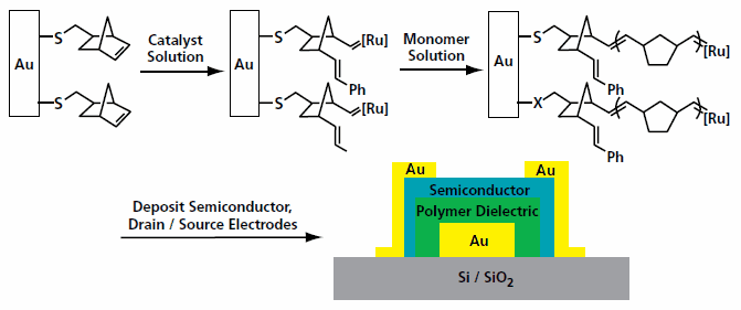
The dielectric layer for organic transistors should be as thin as possible, pinhole-free, and ideally with a high dielectric constant for low voltage operation. A well-ordered densely packed SAM may be the thinnest possible high quality dielectric layer. As shown in Figure 1, a SAM is used as the active dielectric layer for high performance low voltage organic transistors.2 Other SAMs, as well as self-assembled multilayers, have also been reported as high performance dielectric layers Figure 2.7,8 SAM initiators have been used for initiating surface polymerization to form dielectric layers Figure 3.9

Figure 2. Schematic representation of the components of an OTFT showing the molecular structures of various organic semiconductors (left) and selfassembled nanodielectries I-III (right). Nanodielectric layers were deposited from solutions of silane precursors.

Figure 3.Modification of a gold gate electode for the surface initiated polymerization reaction to grow a dielectric layer.
Semiconductor layer
To facilitate charge transport, the organic semiconductor layer usually comprises of pi-conjugated oligomers or polymers, in which the pi-pi stacking direction should ideally be along the current flow direction. This requires the semiconductor molecules to self-assemble into desirable orientation upon either vapor or solution deposition. These well-ordered molecular layers can be formed by (1) proper molecular design of chemical structures that favor crystallization into large ordered domains or (2) self-assembly into mono and multi layers.10,11
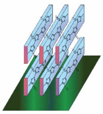
Regioregular poly(3-hexylthiophene) is one of the few polymer semiconductors that spontaneously assemble into well ordered structures upon solution deposition by drop casting or spin coating Figure 4.12 It is among the few reported polymer semiconductors with a mobility greater than 0.1 cm2/ Vs.13,14

Figure 4. Regioregular poly(3-hexylthiophene) spontaneously assemble into ordered structures upon solution deposition. The pi-pi stacking between polymer chains facilitates change transport.
Layer-by-layer deposition is a potentially useful method for organic semiconductor deposition. It allows precise control of the layer thickness, roughness, chemical composition, and molecular orientation. This method has been used to prepare self-assembled multilayers of copper phthalocyanine derivatives. Ion-assisted doping has been observed for these devices.11
Self-assembled monolayers for patterning
For organic transistors, the active semiconductor layer has to be patterned in order to minimize cross talk between devices. Additionally, both the drain and source electrodes need to be patterned so that they are separated by at most a few micrometers depending on application requirements.
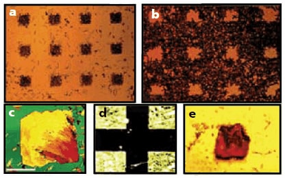
In addition to various printing methods, such as ink-jet printing, screen printing, and offset printing,15-17 SAM modified surfaces have been used for selective deposition of organic semiconductors through patterned wettability or templated growth Figure 5.18,19 Patterned SAM layers can be patterned by conventional photolithography or microcontact printing.20 In addition to pattern organic semiconductors, patterned SAM can be used as an etch resistant layer to prevent etching of an Au film underneath a thiol SAM to generate Au electrodes.21 Patterned SAM layers have also been used to initiate electroless plating of patterned metal electrodes on plastic substrates.22

Figure 5. Optical micrographics of patterned arrays of organic semiconductor crystals nucleated selectively on to self-assembled terphenyl thiol template patterens: (a) and (b) anthracence crystals, scale bar = 200 mm; (c) large oriented sigle crystal of anthracene, scale bar = 50 mm (d) patterned anthrancene crystalline films, scale bar = 300 mm; (e) patterned single crystal of 5-chlorotetracence, scale bar = 100 mm
In summary, both self-assemblies and self-assembly processes are crucial as active materials as well as low cost fabrication methods for organic flexible electronic devices. Significant progress has already been made in this field. Nevertheless, as the demand for performance and precision in patterning increases, self-assembly processes will become increasingly important.
References
To continue reading please sign in or create an account.
Don't Have An Account?